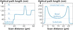
A group of researchers from the Australian National University (Canberra) and the University of Wisconsin (Madison) has discovered that a single molecular layer L of molybdenum disulfide (MoS2) has a giant optical path length (OPL); in comparison to another monolayer material, graphene, the OPL of MoS2 is about 10 times greater. Although this may seem like an esoteric result, it has a very practical consequence for photonics: as the researchers have demonstrated, just a few monolayers of MoS2 can be used to create what the researchers call the “world’s thinnest optical lens,” only 6.3 nm thick. With a diameter of about 20 μm, the concave MoS2 lens the researchers fabricated has a calculated focal length of −248 μm at a 535 nm wavelength.
For experimentation, the researchers transferred single- or few-layer MoS2 flakes onto a silicon wafer (under a microscope, regions of differing colors corresponded to layers of different thickness). To create the lens, they used a focused ion beam to mill a concave bowl shape, producing a continuous, curved OPL profile. The giant OPL arises from a corresponding giant elastic photon scattering efficiency. The researchers discovered that the strength of the elastic interaction in the thin 2D MoS2 increases greatly with a growing refractive index as a result of the ultrathin-film geometry. For every layer thickness increase of 1 nm, the OPL increases by more than 50 nm. The researchers say that other high-index ultrathin-film transition-metal dichalcogenide 2D semiconductors (of which MoS2 is an example) are particularly well-suited for this approach. Reference: Jiong Yang et al., arXiv:1411.6200 [cond-mat.mtrl-sci] (2014).
