Indium phosphide addresses 10-Gbit/s metro demand
By Hava Volterra
The low cost and increasing maturity of metropolitan optical networking systems have made metro systems increasingly attractive for intermediate distances of 300 to 500 km, previously the exclusive domain of long-haul systems. To address these distances, as well as for shorter distances of 40 to 300 km, metro system manufacturers require highly compact, cost-effective active components with superior transmission performance.
Indium phosphide (InP) modulators have been commercially available for more than five years in wavelength-division multiplexing (WDM) and single-channel transmission, in the form of electroabsorption modulated lasers (EMLs) that incorporate the laser and modulator in one package. While these devices were initially used only at 2.5 Gbit/s and for shorter-distance 10-Gbit/s transmission, they are increasingly being used for 10-Gbit/s transmission over longer distances.
Today's EMLs can transmit to distances of 60 km. Achieving 80-km transmission with full International Telecommunications Union (ITU) grid coverage, however, is still a significant challenge because of spotty availability and higher costs. Stand-alone electroabsorption modulators (EAMs) along with a standard distributed-feedback (DFB) or tunable laser offer better availability and performance. For applications where the small size of an EML is ideal, hybrid devices that incorporate an electroabsorption modulator and a DFB laser in an EML-size package are compelling.
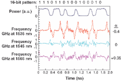
Indium phosphide EAMs share with other InP devices the advantages of high bandwidth and low drive voltages. The 10-Gbit/s versions of InP EAMs are similar in structure to those used for 40-Gbit/s transmission, and regularly surpass 15 GHz in bandwidth. They can therefore generate a high-quality optical eye, and operate well in systems utilizing high bandwidth forward error correction (FEC) at 10.7 Gbit/s and higher (see Fig. 1).
A common measure of modulator performance is chirp. Electroabsorption modulators feature an adjustment that enables achievement of zero or even negative chirp through changes of bias voltage. Alternatively, at a constant bias voltage, the EAM can maintain low chirp over a wide spectral range, enabling high performance transmission with a single device over a wide spectral range (see Fig. 2).
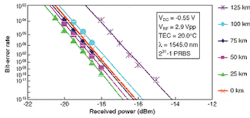
The ultimate test of modulator performance is the transmission results that are achieved with it. A 10-Gbit/s EAM can transmit, error free, at distances up to 125 km, with a dispersion penalty of under 2 dB. This performance is comparable to the performance achieved with lithium niobate (LiNbO3) modulators, and is more than adequate for distances of 500 km and beyond (see Fig. 3).
EAM Alternatives
There are three different forms of EAMs. The first, as described above, is a stand-alone device. A stand-alone EAM combines the advantages of superior performance, with the ability to connect to a variety of laser sources, including tunable sources. It is well suited to the most demanding metro applications. On the other hand, because two separately packaged devices are used, the solution is slightly bulkier than hybrid or monolithic solutions.
The second is a monolithic device, incorporating both laser and modulator on the same indium phosphide (InP) chip. This device is commonly called an EML (electroabsorption-modulated laser) The EML is highly compact, but integration of the laser with the modulator on the same InP substrate involves several compromises. The first is that performance of each of the separate elements (DFB laser and EAM) is not optimal, due to the requirement to grow both on the same substrate. The second, also related to dual device performance, is that yield is reduced, resulting in higher prices. The third is that interaction between the EAM and DFB (specifically reflection of light from the EAM back into the DFB) causes chirp and further reduces transmission performance. The fourth is that producing EMLs at each of the WDM ITU grid wavelengths is an operational challenge. Despite these compromises, EMLs have made significant inroads in shorter reach 10-Gbit/s WDM transmission. If their performance and availability problems were overcome, they could become dominant in longer reach applications as well.
The third alternative is a hybrid device, with laser and modulator integrated in one package. This device can offer the performance and availability advantages of the stand-alone EAM, in the highly compact package of an EML. The package and electrical characteristics of this device are identical to an EML. However, this device does not suffer the performance and manufacturing compromises of a monolithic EML. The DFB laser and EAM are grown separately on separate InP wafers, allowing each one to be optimized independently of the other (see "How do indium phosphide electroabsorption modulators work?" on p. 64). The DFB laser can be independently selected, making matching to the ITU grid much easier. An isolator placed between the DFB and the EAM eliminates reflection effects between the laser and the modulator. Overall, cost is reduced and performance is enhanced (see Fig. 4).
Several evolutionary steps will, over time, enhance and expand the applications and ease of use of the hybrid EML. Primary steps include: integration of drive electronics into the EML package to reduce overall design and manufacturing expense and reduce transmitter size; integration of wavelength locking for dense WDM applications; allowing channel spacing of 50 GHz and below without use of an external wavelength locker; and incorporation of tunable lasers to provide easier sparing and to address switching and crossconnect applications. In addition, amplification can be added into a hybrid EML, allowing higher launch powers out of the device and reducing the cost and extra size associated with post amplifiers.
HAVA VOLTERRA is vice president of sales and marketing for CyOptics, 159 Overland Road, Waltham, MA 02451; e-mail: [email protected].
How do indium phosphide electroabsorption modulators work?
Indium phosphide (InP) is a member of the III-V family of semiconductors. The III-V materials are binary crystals with one element from the metallic group "III" on the periodic table (in this case indium), and one from the nonmetallic group "V" (in this case phosphide). Other members of the family include gallium arsenide (GaAs), indium antimonide (InSb), and indium arsenide (InAs).
Indium phosphide has been the focus of development since the early 1980s, and today the material is being used as a platform for a wide variety of fiber communications components, including lasers, LEDs, semiconductor optical amplifiers, modulators, and photodetectors.
Some InP "quaternaries"including indium gallium arsenide phosphide (InGaAsP)share the same lattice constant as InP, allowing epitaxial growth on top of the basic InP wafer. They are often grown as part of the InP laser or modulator, and provide attributes such as electrical confinement to improve laser efficiency and optical confinement to provide active (gain or absorption) or passive (transparent) optical waveguide functions. Other nonmatched materials may also be grown in thin layers to add useful properties such as quantum effects and strain. Because the refractive index of InP is high, very compact optoelectronic devices can be made.
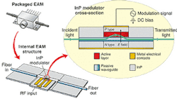
In the internal structure of an InP electroabsorption modulator (EAM), light is coupled from the fiber into the modulator waveguide. From there, it moves to the active region, where the electrical signal causes the modulator to act as an electronic shutter. It then moves on to the output waveguide, and from there to the output fiber. A distributed feedback (DFB) laser can be inserted in lieu of the input fiber to create a hybrid electroabsorption modulated laser of high performance and compact size.
An electro-absorption modulator (EAM) uses the Franz-Keldysh effect in InGaAsP. When no electrical field is present, the InGaAsP material is transparent. The material absorption coefficient increases dramatically when an electrical field is present, turning the EAM opaque to incoming light, effectively acting as an electronic shutter or modulator.
An EAM chip consists of three sections: one active section with two passive sections on each side (see figure). The passive sections contain only passive waveguides, used to transition the light from its shape in optical fiber to the material characteristics of the InGaAsP. The active section acts as a diode in reverse bias. Light is coupled from the input fiber into the waveguide and from there into the active region, where it is modulated, and then into the output waveguide and out to the output fiber.


