Birefringence in calcium fluoride is mapped in two dimensions
Researchers at Hinds Instruments (Hillsboro, OR) presented 157-nm birefringence maps of calcium fluoride (CaF2) samples at International Sematech's 157-nm Technical Data Review (May 7-9; Dallas, TX). Bob Wang of Hinds showed two-dimensional (2-D) images as well as contour maps displaying both magnitudes and corresponding fast-axis angles of both residual and the recently discovered intrinsic form of birefringence in CaF2 at 157 nm.
In May 2001, researchers at the National Institute of Technology and Standards (Gaithersburg, MD) reported unsuspected high levels of intrinsic birefringence in CaF2 based on single-point measurements of multiple samples, levels that can severely affect lens design and images. The new 2-D birefringence maps of the entire surfaces of CaF2 cubic samples measured in the [110] orientation revealed significant variation in birefringence, possibly due to residual birefringence in those samples; lower levels were also observed for the [001] orientation. One proposed design solution is to couple lenses in the imaging system at offsetting orientations. Wang validated this approach, presenting data from two 1-in. stacked cubes in the same orientation [110]; when one of the cubes was rotated by 90°, the total mean birefringence was reduced from 54.64 to 0.87 nm. Contact Bob Wang at [email protected].
Enter the braggoriton
In studying synthetic opal three-dimensional photonic crystals (PCs) infiltrated with a highly polarizable medium, researchers at the University of Utah (Salt Lake City, UT) and the University of Texas at Dallas (Richardson, TX) have, in this special case, found excitations present within the photonic bandgap, dubbing them "braggoritons." The effect is to split the Bragg-reflectivity plateau in two, leaving a partially transmitting spectral region in between.
The PC was produced by mixing a colloidal suspension of 300-nm-diameter silica spheres and letting them form a sediment, then sintering the resulting face-centered cubic structure at 750°C. A solution of cyanine dye in chloroform was infiltrated into the PC, causing the dye molecules to form aggregates with greatly reduced photoluminescence. The researchers took reflectivity measurements both with and without dye molecules along the crystal's [111] direction, which has the most distinct stop band. Though disorder in the crystal smeared out spectral features, a split in the reflectivity spectrum (or, looking at it another way, the introduction of a second peak) was seen as the incidence angle was reduced-the rise of the braggoriton. Contact Zeev Valentine Vardeny at [email protected].
Optical fiber transmits 11 kW of COIL light
As a result of its scaling properties and favorable wavelength (1.3 æm) for optical-fiber transmission, chemical oxygen iodine laser (COIL) technology offers major advantages for the decommissioning and dismantling of nuclear installations. One key element to successful industrial application is the demonstration of high-power fiber transmission. This has been achieved using the COIL facility at the Aerospace Research Center (Lampoldhausen, Germany).
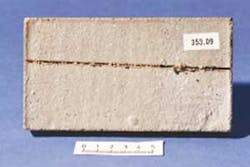
The laser was operated with a stable resonator and the beam was collected using an aperture-limited lens in order to block residual high-divergence radiation. Alignment was first established with a helium-neon laser and subsequently fine-tuned using an infrared camera to position the focal spot onto the end of the fiber. The laser radiation was coupled into a 1-mm-core, 0.2-numerical aperture fiber through an antireflection- coated lens system designed in cooperation with Highyag (Stahnsdorf, Germany). An average power level of 11 kW was successfully transmitted through the 20-m-long fiber with total losses between 10% and 15% after the end effector. Efficient laser cutting was demonstrated for several pertinent materials, including concrete (shown here), aluminum, and graphite. Contact Willy Bohn at [email protected].
Gallium nitride-based LEDs on silicon show benefits
Fabricating gallium nitride (GaN)-based light-emitting diodes (LEDs) on silicon (Si) substrates rather than on sapphire or silicon carbide has more than one potential benefit-a fact that has stimulated two groups of researchers to pursue two very different goals. The first group, at Texas Tech University (Lubbock, TX), is growing GaN-based ultraviolet-emitting devices by gas-source molecular-beam epitaxy, aiming to take advantage of the shorter wavelengths made possible by fabrication on Si. The LEDs emit at peak wavelengths between 325 and 350 nm, some with full-width-at-half-maximum widths of only 11 nm. The devices would be especially useful for fluorescence- and absorption-based detection systems. Contact Sergey Nikishin at [email protected].
The second group, at Otto-von Guericke Universität (Magdesburg, Germany), intends to lower the cost of blue-emitting LEDs by eliminating expensive substrates. The researchers have grown entirely crack-free GaN-based LEDs on 2-in. Si wafers using metalorganic chemical-vapor deposition. The devices emit at 152 æW at 20 mA and 455 nm; optimizing will lower series resistance and raise power. Contact Armin Dadgar at [email protected].
Poled polymer measures fem tosecond electromagnetic pulses
Ultrashort electromagnetic pulses with wavelengths in the terahertz and infrared region have potential use in nonlinear spectroscopy. Scientists at Columbia University (New York, NY) and NEC Research Institute and Princeton University (both of Princeton, NJ) are using poled polymers to detect these kinds of pulses. The material enables coherent detection of radiation ranging from the far-infrared to the mid-infrared (33 THz) regions.
To generate the radiation, the beam from a modelocked Ti:sapphire laser producing 23-fs pulses was focused onto a gallium arsenide wafer to produce the pulses by optical rectification; the ultrashort pulses were then refocused by two off-axis paraboloidal mirrors. A 35-æm-thick layer of nonlinear polymer was deposited on a metal layer acting both as an electrode and a mirror that doubles the optical interaction length. The detected waveform was a decaying oscillation with femtosecond structure and an oscillatory tail. Phase-matching in the poled polymer was important for a broad spectral response; high-frequency response was limited by absorption in the polymer and the duration of the optical pulses. Other choices of chromophore and host matrix will extend the detection bandwidth. Contact Ajay Nahata at [email protected].
Capacitive sensor gets help from optical interferometer
Micromachined capacitive acoustic transducers can be used as miniature microphones as well as for nondestructive testing and ultrasound imaging. But standard devices are electrically noisy, especially in the megahertz range, which limits sensitivity. Now Levent Degertekin, Neal Hall, and Wook Lee of the Georgia Institute of Technology (Atlanta, GA) have integrated an optical interferometer into a capacitive transducer, using applied voltage to deflect the membrane electrostatically to keep the detection sensitivity at the optimum level as well as to send transmission signals for ultrasonic applications.
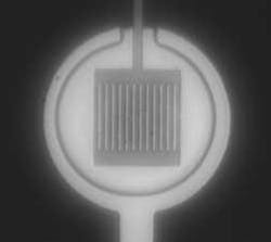
The back electrode of the transparent substrate was formed as a diffraction grating; the intensity of the reflected diffraction orders (sensed by a silicon photodetector) determined membrane displacement. Sensitivity to sensor location was eliminated by taking the relative amplitudes between multiple orders. The light source was either a helium neon laser or an 850-nm-emitting vertical-cavity surface-emitting laser. A scanning electron micrograph shows a 100-æm device on quartz (left), while an optical micrograph reveals an electrode with a diffraction grating (right). A 19 × 19 array of the devices was tested at 750 kHz with good results. Contact Levent Degertekin at [email protected].
null
Off-resonance Raman generation produces wide spectrum
Researchers at Stanford University (Palo Alto, CA) have taken the off- resonant Raman generation technique and applied it to rotational transitions in low- pressure molecular hydrogen, producing a Raman spectrum extending from 1.37 æm to 352 nm and con-sisting of 37 coherent sidebands spaced by 587 cm-1. In the technique, two single-mode lasers with a frequency difference slightly detuned from the Raman resonance generate a comb of sidebands. The conversion efficiency was nearly 100%.
Two Ti:sapphire lasers emit 60-mJ transform-limited pulses at 797 and 836 nm. The tunable wavelengths are monitored by a wavemeter with a resolution of 50 MHz. The synchronized pulses are combined at a dichroic mirror and focused into a hydrogen-filled cell to a peak intensity of 2 GW/cm2. Cooled to 77 K, the cell is set to a pressure of 250 Torr. When laser pulses are applied, bright white light exits the cell, which can be dispersed by a prism and projected onto paper to see the Stokes and anti-Stokes sidebands (these images were taken at three different exposure durations). Pumping with frequency-doubled Ti:sapphire lasers would extend output wavelengths to 250 nm. Contact Steve Harris at [email protected].
null
Research effort produces high-quality UV mirrors
A study conducted by researchers at the Centre National de la Recherche Scientifique (Marseille, France) and the Fraunhofer Institut für Angewandte Optik and Feinmechanik (Jena, Germany) undertakes to design and fabricate better-quality multilayer mirror coatings for the ultraviolet (UV) region. As part of the study, the researchers have characterized single thin-film layers of silica and hafnia, and have made multilayer mirrors containing the two materials that reflect 99% at 300- and 250-nm wavelengths.
Two fabrication techniques-ion plating (IP) and plasma ion-assisted deposition (PIAD)-were found to produce high-grade, dense mirrors for the UV region. The layers produced by PIAD were found to be homogeneous within a thickness range of 30 to 100 nm, with no dependence of refractive index on film thickness. Both techniques produced refractive indices close to that of bulk cubic hafnia, with IP producing a slightly higher value. A 23-layer mirror with a total stack thickness of 0.95 æm had a bandwidth of 45 nm. No changes due to water adsorption and desorption when shifting to and from air to vacuum were seen. Contact Philippe Torchio at [email protected].
Photonic-crystal VCSEL shows single-mode operation for all currents
Researchers at the Korea Advanced Institute of Science and Technology (Taejon, Korea) have fabricated vertical-cavity surface-emitting lasers (VCSELs) that incorporate a photonic crystal (PC) into their active structure to achieve single- transverse-mode beam quality. The two-dimensional PC consists of an array of holes in the laser's top-mirror region, with a single missing hole at the center to create a crystal defect. The PC has a lower effective refractive index than the defect, containing light within the defect.
The gallium aluminum arsenide-based VCSEL emits at 850 nm. The laser's 80- to 86-æm-diameter mesa is etched through 14 to 17 of its 24 high/low-index-layer pairs. The pitch of the etched holes ranges from 5 to 10 æm, while the ratio of hole diameter to hole pitch ranges from 0.3 to 0.6 for different devices. A laser with hole diameter of 5 æm and ratio of 0.6 showed single-mode lasing for all electrical input currents. Similar VCSELs that included oxide apertures were fabricated; some PC hole geometries resulted in a single mode, while others showed multimode operation. One device emitted 0.57 mW of continuous-wave single-mode light. Contact Dae-Sung Song at [email protected].


