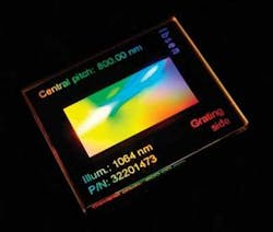
Conventional diffraction gratings are typically replicated in polymer from high-quality and expensive master gratings. Because many polymers are not optically suited for transmission and have poor thermal stability and limited lifetime, these replicated gratings are usually coated with metals and used in reflection mode. But by taking conventional photoresist-patterning techniques one step further and using semiconductor-etching technology, scientists at Ibsen Photonics (Farum, Denmark) are fabricating low-cost, high-quality transmissive diffraction gratings in fused silica, taking advantage of silica’s optical transparency from the deep-UV to the near-IR, its high-temperature and long-lifetime performance, and its close to 100% diffraction efficiency even with high grating resolution and line spacings from 450 to 3000 lines/mm.
The Ibsen technique uses a holographic stepper to first fabricate a grating pattern in photoresist, but transfers the pattern to bulk silica with a reactive ion-etch process that produces a 100% dielectric component free of both polymers and metals. These fused-silica diffraction gratings are particularly suited to laser-pulse-compression applications (where high-power tolerance is required), as well as to more compact spectrometer designs due to their transmissive mode of operation. Contact Torben Jacobsen at [email protected].
About the Author
John Wallace
Senior Technical Editor (1998-2022)
John Wallace was with Laser Focus World for nearly 25 years, retiring in late June 2022. He obtained a bachelor's degree in mechanical engineering and physics at Rutgers University and a master's in optical engineering at the University of Rochester. Before becoming an editor, John worked as an engineer at RCA, Exxon, Eastman Kodak, and GCA Corporation.
