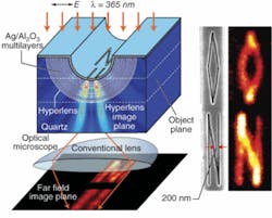
A previously postulated cylindrical-metamaterial optical lens called a hyperlens (see www.laserfocusworld.com/articles/277169) has now become a reality; it images sub-diffraction-limited objects in the far field.1 The lens, which was fabricated by a group of scientists at the University of California, Berkeley (UC Berkeley), is cylindrical and thus images only in one dimension. Objects placed against the cylinder’s inner wall (in the near field) are magnified and imaged on the cylinder’s outer wall to a size above the diffraction limit; a conventional far-field optical system then further magnifies the object.
The inner radius of the experimental cylinder is 450 nm; the wall of the cylinder is made of a periodic stack of 16 layers of silver alternating with 16 of aluminum oxide. Each pair of layers is 70 nm thick, making the cylinder’s outer radius about 1.57 µm (these parameters are flexible, making larger or smaller lenses possible). In the resulting metamaterial, the scattered evanescent field from an object travels within the medium in the radial direction; the structure of the material compresses the tangential wave vectors as the field travels outward, magnifying the image.
To test the hyperlens, the researchers created a sub-diffraction-limited object pattern in a layer of chromium on the cylinder’s inner wall. The pattern consisted of a pair of 35 nm transmissive lines spaced 150 nm apart; a second pattern consisted of the elongated letters “ON” in 40 nm lines. (The second pattern, while nominally two-dimensional, was only of sub-diffraction-limit size in one dimension-the dimension magnified by the hyperlens.) The image on the outer wall was further magnified by a microscope objective with a numerical aperture of 1.4. The researchers also created a control experimental device without the metamaterial.
While the control setup could not resolve the sub-diffraction-limited line pair at a 365 nm illumination wavelength, the hyperlens easily resolved the lines. In addition, the hyperlens sharply distinguished the sub-diffraction-limited features of the “ON” object (see figure).
Researcher Zhaowei Liu notes that the UC Berkeley group will be focusing primarily on improving the lens itself-its performance and reliability-while leaving its possible application to others. The group recently created a spherical version of the hyperlens, which images in two dimensions and works well, notes Liu; the researchers are preparing a paper on the new results. With its greater functionality than the 1-D version, a spherical hyperlens could become a widely used accessory for biomolecular imaging, and possibly for nanolithography.
REFERENCES
1. Z. Liu et al., Science 315, 5818 (March 23, 2007).

John Wallace | Senior Technical Editor (1998-2022)
John Wallace was with Laser Focus World for nearly 25 years, retiring in late June 2022. He obtained a bachelor's degree in mechanical engineering and physics at Rutgers University and a master's in optical engineering at the University of Rochester. Before becoming an editor, John worked as an engineer at RCA, Exxon, Eastman Kodak, and GCA Corporation.