It's hard to believe that digital electronic computers have been around for half a century now, yet it's harder to believe how far these computers have evolved in that time. When ENIAC first glowed to life at the University of Pennsylvania in 1946, it contained 18,000 vacuum tubes, took up an entire room, and could grind out 4500 additions per second. Today, pocket calculators have far more computing power than ENIAC ever did, and supercomputers can zip through billions of calculations per second.
Much of the credit for this spectacular growth goes to the inventions of transistors and integrated circuits, which enabled the higher efficiency and miniaturization of electronics. But as electronic hardware nears the practical limit of size and efficiency, the future growth rate of computing power will rely increasingly on unconventional technologies now under development. One of the most promising of these new technologies is optical computing.
Optical methods offer a radically new approach to computers because the information carriers are photons, which behave very differently from electrons. For example, photons can pass through each other like ghosts; electrons cannot. Photons can also move readily through open space, whereas electrons generally must be routed through conduits. Unlike electrons, photons also carry no charge and are therefore immune to interference from extraneous electromagnetic fields.
These properties provide optical computers with certain potential advantages over the conventional electronic variety, which is why research on optical logic circuits and computer architectures has accelerated in recent years. This article reviews the fundamental design and function of several devices used for optical computing.
Digital electronic computers basically consist of a large collection of interconnected switches, gates, and memory elements called “flip-flops.” Logic operations are performed by controlling the flow of electrons between these various components. Optical computers also use switches, gates, and flip-flops in their logic operations, but the designs of these devices are very different.
The purpose of a switch is to make or break a connection between one or more transmission paths. If a switch controls the connection from just one path to another path, it is called a 1 × 1 switch. Other possibilities include 2 × 2, 1 × n, n × n, and n × m switches, where n and m can be any integer.
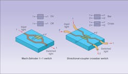
In optical computers, switches can be built from modulators using opto-mechanical, electro-optic, acousto-optic, magneto-optic, and other techniques. For example, a Mach-Zehnder interferometer in which the refractive index of one leg is electro-optically controlled can serve as a 1 × 1 optical switch (see Fig. 1, left). By modulating the relative phase of the divided wavefronts as they pass through the interferometer, they can be constructively or destructively recombined at the output, thus creating an on or off condition.
Another useful optical switching design is the directional coupler, which makes an ideal 2 × 2 switch (see Fig. 1, right). Electro-optic control of the refractive index of these devices shifts them between two states: cross and bar. In the bar state, inputs 1 and 2 are directed to outputs 1 and 2, respectively; in the cross state, inputs 1 and 2 cross over to outputs 2 and 1, respectively. This type of switch is referred to as a crossbar switch and can be expanded to accommodate n × n configurations.
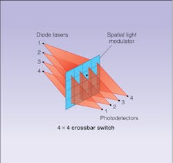
Crossbar switches are an important element of many optical logic circuits and can be fabricated in a variety of ways. For instance, a 4 × 4 crossbar switch can be constructed using an array of magneto-optic modulators (see Fig. 2). In this particular device, light from each diode laser in a vertical array is spread by a cylindrical lens in a fan-like pattern across each row of the 4 × 4 spatial light modulator (SLM). Another set of cylindrical lenses (oriented orthogonally to the first set) then focuses the light passing through each column of the SLM onto a corresponding detector of a horizontal detector array.This optical configuration can connect any input line (diode laser) with any output line (detector) without conflict. If all of the modulators of the SLM were open, for instance, then each input line would be individually connected to all of the output lines. However, connecting input line 2 only with output line 3 means closing all modulators of the SLM except the one in the second row, third column (marked by a dot in the figure). Many other combinations are possible, of course.
In principle, the magneto-optic SLM of a crossbar switch can be replaced by a liquid-crystal SLM or even an acousto-optic SLM. These and other optical modulator technologies have been developed into larger n n switches for more computing power. Acousto-optic modulators also are well suited for 1 × n and n × m optical switching. However, all of the optical switches described so far are electrically or magnetically controlled. With the help of certain nonlinear optical effects, though, all-optical switches can be constructed as well. (For a brief overview of nonlinear optical effects, see Back to Basics, August 1994, p. 67).
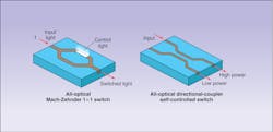
Using the optical Kerr effect, for example, it is possible to transform both the Mach-Zehnder interferometer and directional coupler into all-optical switches. In each case, a strong beam of light (not an electric field) affects the switch behavior.
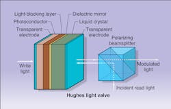
If a bright control beam passes perpendicularly through one leg of the Mach-Zehnder interferometer, the refractive-index change caused by the optical Kerr effect creates the relative phase shift needed to operate the switch (see Fig. 3, left). But a single beam coupled into just one of the waveguides of a directional coupler can convert this device into a self-controlled switch (see Fig. 3, right). When the beam is bright enough to raise the refractive index of the input waveguide of the coupler, the light remains confined to the same waveguide. If, however, the beam intensity is low, the coupler operates normally by channeling the light into the adjoining waveguide. This switch can be used to separate strong and weak signals from a data stream.Optically addressable light valves such as this one can perform as all-optical switching arrays (SLMs) for parallel processing. In fact, all-optical switches are critical components in optical computers because they are directly cascadable, which means they can be linked so that the light output of one device becomes the input of another. Cascadability is a crucial element of logic circuits.
Bistable switches and flip-flops
The optical output of a single switching device can also be fed back to the same device. If the optical medium of the switch behaves nonlinearly, the feedback will create a condition in which the switch can assume only one of two stable states. Bistable optical switches are very important to optical computing because they can function as flip-flops.
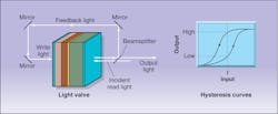
To illustrate the flip-flop function, an optically addressed liquid-crystal light valve can be converted into a bistable switch by rerouting a portion of the reflected light output to the write side of the device, which is normally addressed by an independent light beam (see Fig. 5, left). This arrangement creates a bistable condition because the reflectance on the read side of the light valve is a nonlinear function of the feedback intensity to the write side. The result is a characteristic hysteresis between the output and input intensities (see Fig. 5, right).Under the right conditions, hysteresis can endow the switch with a kind of memory whereby the output depends on previous conditions. The trick is to bias the device with an input intensity that falls midway between the two stable states (I? in the figure). From this bias condition, the output intensity can be made to flip-flop between the high and low stable states; however, the exact behavior depends on prior events.
For example, the switch will latch into the high-output state if the input briefly surges far enough above the bias level. But if the switch is already in the high-output state, it will remain in that state when the input surges. A momentary drop in the input bias level, however, will latch the switch into its low-output state. This kind of behavior defines a flip-flop.
Many other bistable optical switches have been developed as well. These include Mach-Zehnder interferometers and Fabry-Perot etalons, in which optical feedback induces the Kerr effect; hybrid bistable switches, in which the feedback is electronic rather than optical; and Fabry-Perot etalons with saturable-absorber cavities. But one of the most promising bistable optical switches is the self-electro-optic-effect device, or SEED.
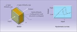
A SEED consists of a stack of heterostructure multiquantum-well semiconductor layers with a bias voltage across it (see Fig. 6, left). The optical absorption of such a structure is a nonlinear function of the voltage applied across it. But the charge carriers generated when light passes through the layers also affect the absorption and provide the internal feedback mechanism needed for bistability. Because absorption increases rapidly above a certain input intensity, the hysteretic response of SEEDs is inverted. Therefore output intensity drops to the low state when input intensity surges above the bias voltage and vice versa (see Fig. 6, right).An important variation of the SEED is the symmetric SEED (S-SEED), which is formed by connecting two SEEDs together in series. S-SEEDs function as flip-flops that respond to the relative intensity between two input beams. These and other SEED designs can be fabricated into high-density switching arrays that can perform with very high gain, relatively high speed, and very low energy.
Interconnections and architectures
In any computer, the various components must be integrated into an architecture designed to perform some logical function. The function can be specific, such as adding one set of numbers to another, or it can be general and programmable.
Almost all of the digital electronic computers in use today emulate the sequential architecture laid down by John von Neumann (1903-1957) in 1953. Sequential computers grind through a set of logical operations one step at a time. The primary advantage of optical computers is that they can be naturally configured into parallel architectures in which many operations are performed at once.
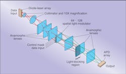
A good example of parallel architecture can be found in the digital optical computer (ODOC IIO) built by OptiComp Corp. (Lake Tahoe, NV). This digital computer combines linear arrays of diode lasers and avalanche photodiodes (APDs) with anamorphic optics and an acousto-optic SLM to perform programmable Boolean logic operations (see Laser Focus World, Aug. 1994, p. 77). Specifically, the computer functions as a Boolean-logic matrix/vector multiplier in which the combinatorial functions are computed in parallel.
To accomplish this, electronic data are fed into a linear array of 64 individually addressable diode lasers (see Fig. 7). The data are coded in 32-bit binary form (0?s and 1?s) where each bit, x, is accompanied by its logical complement, x?. The binary complement of a 1, for example, is 0 and vice versa. On the laser array, each bit and its complement appear as a pattern of high and low intensities. This represents the data vector.After collimation and magnification, a series of cylindrical lenses then spreads the light from each laser element across each row of an acousto-optic SLM consisting of 64 rows and 128 columns. The SLM acts as a two-dimensional control mask by selectively passing (diffracting) or blocking (zero-order diffraction) the laser light through each element of the modulator array. This step is the mathematical equivalent of multiplication, which in Boolean logic is represented by the AND function. Thus the SLM multiplies the data bits from the linear laser array by control bits, which are fed into the SLM electronically.
A second set of cylindrical lenses then takes the light pattern passing through each column of the SLM and focuses it onto a corresponding detector in a 1 × 128 horizontal APD array. This step is mathematically equivalent to addition, which is represented by the OR function in Boolean logic. Because each detector of the array is reversed-biased, the electronic signal it generates is inverted from the positive light signal, which is equivalent to the NOT function in the Boolean system.
By combining AND, OR, and NOT functions, any logical operation can be performed in the Boolean system. Thus, DOC II is a fully programmable, general-purpose computer in which programming is done through the SLM. More important, processing also is done in parallel through the optical interconnections and the SLM.
Many other computer architectures have been designed that exploit the innate parallelism of optics. For example, OptiComp Corp. is developing DOC III, which uses global interconnects and advanced optoelectronic integration for massively parallel computing. Global interconnects use diffractive optics such as holograms to link each element of a two-dimensional array to all elements of another array or vice versa.
Optical computers need not be digital, either. There are analog and multi-valued-logic architectures, as well as optical cellular automata, optical dataflow machines, and linear and nonlinear optical neural networks.
All of these developments underscore the extraordinary versatility of electro-optics. From the simplest lens to the most intricate optical computer, electro-optic technology has already enriched our lives beyond measure, and many exciting developments are expected in the decades ahead.
ACKNOWLEDGMENT
The following people provided important background information for this article: John Hessenbruch, David McCallum, and Richard Stone of OptiComp Corp.
FURTHER READING
Alastair D. McAulay, Optical Computer Architectures: the Application of Optical Concepts to Next Generation Computers, John Wiley & Sons, New York, NY (1991).
Raymond Arrathoon, ed., Optical Computing: Digital and Symbolic, Marcel Dekker, New York, NY (1989).
Dror G. Feitelson, Optical Computing: A Survey for Computer Scientists, MIT Press, Cambridge, MA (1988).
Ravindra A. Athale, ed., Digital Optical Computing, SPIE Optical Engineering Press, Bellingham, WA (1990).
H. John Caulfield and Gregory Gheen, eds., Selected Papers on Optical Computing, SPIE Optical Engineering Press, Bellingham, WA (1989).
L. D. Hutcheson, ed., Integrated Optical Circuitry and Components, Marcel Dekker, New York, NY (1987).
B. A. Saleh and M. C. Teich, Fundamentals of Photonics, John Wiley & Sons, New York, NY (1991).
About the Author
Thomas V. Higgins
Contributing Editor
Thomas V. Higgins was a contributing editor for Laser Focus World, covering science and technology.
