SOL P. DIJAILI and JOHN M. WACHSMAN
The mantra of telecommunications providers—lower cost, smaller size, and lower power—is pushing optical components manufacturers to move quickly toward higher levels of integration. And high levels of integration, either hybrid or monolithic, require chip-based optical amplifiers. Without optical amplification based on chips, integration is limited by the total passive loss that can be tolerated in a single package. This severely limits the size, functionality, and flexibility of optical networks.
The world of optical amplifiers-on-a-chip consists of three types: linear optical amplifiers (LOAs), semiconductor optical amplifiers (SOAs), and gain-clamped semiconductor-optical amplifiers (GC-SOAs). Their basic structures differ in several ways (see Fig. 1). The SOA consists of a bar of indium phosphide (InP) that has an active region, between a p-n junction, biased with a constant current source. This current creates a population inversion allowing amplified stimulated emission of an input optical signal, introduced into the end of the bar. The active region (with a higher index of refraction) is sandwiched between two cladding layers (with a lower index of refraction), creating the amplifier waveguide. The chip itself is then coupled to input and output fibers, typically with lenses or lensed fiber.
The LOA structure integrates mirrors on the top and bottom of the chip to create a vertical-cavity surface-emitting laser (VCSEL) using the same active region. The VCSEL acts as optical feedback and linearizes the amplifier. This method integrates the feedback directly into the amplifier chip itself. The LOA avoids distortion by using the feedback properties of a large supply of ballast photons created by the VCSEL in the heart of the amplifier. Like the keel that ballasts a boat against gusts of wind, the ballast laser perfectly counteracts the tendency of the semiconductor to react to "gusts" of photons—the incoming signal pulses—and ultimately keeps the gain of the amplifier constant, or "linear."
The GC-SOA is similar to the SOA, except that a mirror is placed at either end of the SOA chip. This creates a laser that is used to stabilize the gain of the optical amplifier. In this case, the lasing field is longitudinal, parallel to the direction of the optical signal.
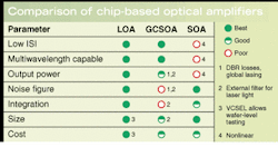
Although the three structures seem quite similar, the linear performance of each amplifier is very different (see table). In addition, the optical feedback mechanism has implications for hybrid or monolithic integration.
Linear performance comparison
The output power capability of a chip-based optical amplifier is one of the most confusing specifications in the industry. Many manufacturers have adopted the definition used by erbium-doped fiber amplifier (EDFA) manufacturers—saturation power (Psat)—defined as the output power at which the gain of the amplifier is compressed by 3 dB. The difficulty with this definition is that chip-based amplifiers, with gain dynamics significantly different from EDFAs, are nonlinear and provide a distorted output waveform when operated at 3-dB gain compression. The SOA, with its high-speed gain dynamics, would react to the individual bits, while EDFAs do not. Therefore, SOA gain is highly dependent on the bit pattern and number of wavelengths traveling through it, a characteristic that easily leads to distortion.
Two types of distortion associated with the output power of the amplifier are symbol interference and wavelength-division multiplexing (WDM) crosstalk. Intersymbol interference (ISI) occurs when the input signal becomes strong enough to deplete the population inversion created by the bias current. A finite recovery time is needed for the bias current to restore the population inversion to the proper level. In an SOA, this time is on the order of 200 ps.
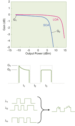
The effects of SOA gain dynamics are noise and distortion of the signal. At the beginning of the first bit, when there is a sufficient population inversion, the gain of the amplifier is G1 (see Fig. 2). However, the strength of the input signal quickly depletes the inversion layer and lowers the gain to G2 by the end of the bit. During the zero bit at time t2, the bias current begins to recreate the inversion, but not before another bit occurs at time t3. So the bit in t3 has a lower average gain than the bit during time t1. Thus, depending on the pattern preceding a given bit, the gain for a given bit will be uncertain and hence noise or symbol interference.
The second type of distortion is WDM crosstalk, which is channel-to-channel crosstalk in a multichannel transmission. The mechanism is similar to that described above, but instead of having two distinct gain values G1 and G2, there are n + 1 states, where n is equal to the number of wavelengths. The term crosstalk is used because the bit pattern of λm gets imprinted on λn and vice versa.
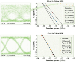
The LOA structure yields a flat gain vs. an output-power curve that provides linear amplification up to an output power of above 10 dBm. The flatness of the curve up to this power level ensures that ISI and multichannel crosstalk are absent (see Fig. 3). For the SOA, the slope of the gain curve experienced by a single data channel causes a receiver penalty of about 1 dB, due to ISI. Adding a second channel enlarges that penalty, which also has contributions from ISI and interchannel crosstalk. Increasing the power in both channels makes the crosstalk penalty so high that an error floor arises, which makes proper data transmission impossible using an SOA. The LOA measured under the same conditions shows no penalty in each of the three cases.
Comparing the LOA and GC-SOA
There are many differences between the LOA and GC-SOA although they both use a laser as optical feedback. The lasing mode is orthogonal for the LOA and longitudinal for the GC-SOA. The significant difference between the two structures is that the mirrors used to create the laser for the GC-SOA are in the optical path, adding loss. Moreover, the lasing signal must be kept from traveling down the input and output fiber. A bandpass filter at the input and output of the amplifier can solve this, but adds loss in the optical path. These additional losses increase the noise figure and reduce the output power of the amplifier.
The LOA structure does not use mirrors in the optical path and the orthogonal nature of the lasers means that the ballast photons do not propagate down the fiber, so bandpass filters are not needed. This allows many LOA structures to be integrated monolithically on a single chip.
The highest performing optical amplifiers use multiple sections. Each individual section focuses on providing the best performance for a given specification. For example, high-performance EDFAs use a 980-nm pump on the input stage to achieve the best noise figure and a 1480-nm pump at the output stage to achieve the highest output power.
The LOA laser is actually a long, skinny VCSEL, but can be thought of as a long series of individual VCSEL lasers. Because the optical feedback is done "locally" along the entire length of the gain medium, it is possible to design the amplifier in sections. To achieve the lowest noise figure, for example, a relatively high lasing-threshold current is important. However, for the best output power, a low lasing-threshold current is best for optimum performance.
By comparison, the longitudinal lasing mode of the GC-SOA clamps the gain in a "global" fashion. This means that the amplifier has only one section. As a result, the design details dictate that gain and noise figures are traded off against each other. Since a higher gain means a lower mirror reflectivity, a higher laser intensity at the ends of the device results, and hence a lower population inversion at the input of the GC-SOA occurs. A lower population inversion at the input end results in a higher noise figure.
The LOA structure uses VCSEL technology proven to have low manufacturing cost. This is because the emissions of the VCSEL light can be measured while the devices are still on the wafer. This eliminates bad die early in the manufacturing process, before the VCSELs are packaged. This is not true for the GC-SOA or SOA—as edge-emitting devices, they must be cleaved, coated, and mounted—a costly process—before the quality of the device is known.
At the time this was written, Sol P. Dijaili was chief technical officer and co-founder, and John M. Wachsman was director of marketing at Genoa, which was recently acquired by Finisar, 1308 Moffett Park Dr., Sunnyvale, CA 94089-1133; e-mail: [email protected].


