Quantum-cascade laser reaches watt-level average powers
A 0.67-W average power for a room-temperature 5.9-µm-emitting quantum-cascade (QC) laser has been demonstrated by researchers at Northwestern University. The group aimed to reduce the devices' threshold current density and their dependence on temperature. They achieved this by increasing the conduction band offset of the heterostructure, lowering the doping in the injector region, and including a thick gold top-contact layer.
A double-channel ridge-waveguide QC structure was grown on an indium phosphide substrate, with compressive gallium indium arsenide and tensile aluminum indium arsenide making up the well and barrier materials. Ridge waveguides of 20-, 27-, and 40-µm widths were fabricated. The 5-µm-thick gold layer was deposited by electroplating; the layer helped remove heat. The cavity was 2 mm long. The threshold current density was 1.7 kA/cm2 for the 20-µm-wide lasers, which operated at an average power of 0.224 W at a 56% duty cycle and 0.521 W at a 28% duty cycle. The 0.67-W average power was reached by the 40-µm-wide device operating at a 17% duty cycle. Contact Manijeh Razeghi at [email protected].
III-nitride microlens arrays may facilitate integration of optoelectronic devices
Researchers at Kansas State University (Manhattan, KS) have fabricated III-nitride microlens arrays for blue and ultraviolet wavelength applications on gallium nitride (GaN) and aluminum nitride (AlN) using photoresist reflow and inductively coupled plasma dry etching. Microlens diameters as small as 10 µm were achieved with focal lengths varying from 7 to 30 µm, as measured by near-field scanning optical microscopy. "The successful fabrication of microlens arrays based on III-nitride materials opens the possibility for monolithically integrating nitride-based micro-sized photonic devices, as well as coupling light into, out of, and between arrays of III-nitride emitters, especially for short wavelengths covering the green-blue to deep-ultraviolet (200-nm) region," says physics professor Hongxing Jiang. In addition to the microfabrication process itself, a major technical challenge was the thin-film epitaxial growth of high-quality AlN. Gallium nitride and AlN epilayers were grown using metal-organic chemical-vapor deposition to a thickness of 3 to 3.5 µm on sapphire substrates with a 30-nm GaN or AlN low-temperature buffer layer. Contact Hongxing Jiang at [email protected].
All-optical sectioning of tissue produces diffraction-limited volumetric images
The conventional way to determine the detailed three-dimensional (3-D) structure of tissue is to freeze it, slice it into sections, and examine or scan the slices with a microscope. This technique is laborious and can affect the tissue's structure. In contrast, an all-optical technique developed by researchers at the University of California, San Diego (La Jolla, CA), Science Applications International (Arlington, VA), and the Colorado School of Mines (Golden, CO) and presented at the Conference on Lasers and Electro-Optics 2003 (CLEO 2003; June 1–6; Baltimore, MD) is highly automated and produces accurate issue scans.
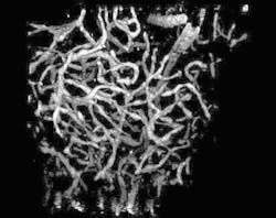
In the technique, a shallow 3-D portion of a fluorescent-labeled sample is imaged by two-photon nonlinear microscopy with a focused femtosecond laser as the light source, providing diffraction-limited imaging over a 150-µm-deep volume. The same pulses at a higher power are then used to ablate the volume away, allowing a similarly sized volume beneath to be imaged; the process is repeated many times. The sharply defined volume borders stitch together seamlessly (aided by software) to produce a large-volume 3-D digital image, as in this 250 × 375 × 400-µm region of a transgenic mouse's neocortex. The surface roughness of the sections is similar to that in conventional frozen sections. Contact Jeff Squier at [email protected].
Implanted carbon forms waveguide in Nd:YAG
Optical waveguides in Nd:YAG crystals are a potential basis for many interesting optoelectronic devices. Researchers at the Centro de Investigaciones en Óptica (Guanajuato, Mexico), the Universidad Nacional Autónoma de México (Distrito Federal, Mexico), and the Universidad Autónoma de Madrid (Madrid, Spain) have produced such waveguides by implanting carbon into Nd:YAG to decrease the index of refraction in the implanted region by 2.5%, then annealing the crystal at 400°C to recover its transparency.
Using a Van de Graaf accelerator, carbon ions with an energy of 7 MeV were implanted into a commercial YAG crystal doped with a 1% Nd concentration. The planar waveguide's low-index barrier was formed at a depth of 4 µm. Thermal annealing increased the waveguide's transparency by a factor of 10. At a wavelength of 632.8 nm, five tightly confined modes were seen, with a sixth mode showing broadening and thus not totally confined. Spectroscopic measurements showed a slight broadening of the Nd emission bands, but the peak positions and the lifetime of 240 µs are similar to those of bulk Nd:YAG. Contact Gloria Verónica Vázquez at [email protected].
Photonic crystals produce negative refraction
Researchers at Bilkent University (Ankara, Turkey) have demonstrated negative refraction of electromagnetic waves in a two-dimensional dielectric photonic crystal with periodically modulated positive permittivity and a permeability of unity. The structure consisted of a square array of alumina rods in air and exhibited its maximum angular range of negative refraction at a 13.7-GHz operating frequency. They observed a negative refractive index of -1.94 after calculating a theoretical value of -2.06 using a finite-difference time-domain simulation. Because the observed negative-refraction effect depends only on the refractive index of the dielectric material and the geometry of the two-dimensional photonic crystal, the researchers assert that the effect can also be observed at optical wavelengths using transparent semiconductors, and that the demonstration represents a step toward developing a lens that will focus features smaller than the wavelength of light. Contact Ertugrul Cubukcu or Ekmel Ozbay at [email protected].
Active-matrix bistable reflective display is inkjet-printed
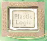
Flat-panel displays typically must be fabricated using a high-precision manufacturing process such as photolithography. Organic and plastic-based displays can potentially be manufactured by inkjet printing of features, a process offering vast reductions in cost. Engineers at Gyricon Media (Ann Arbor, MI) and Plastic Logic (Cambridge, England) have now developed an inkjet-printable bistable reflective display—a type of display especially useful for low-power sunlight-readable applications, and that falls in the realm of "electronic paper."
The display's active-matrix backplane contains polymer thin-film transistors and soluble conductors, with features defined by surface-energy patterning (wettable and nonwettable surfaces). The plastic electronics are compatible with flexible substrates, and ultimately with roll-to-roll manufacture. The liquid-crystal pixels scatter when off and transmit when on. The prototype display has 4800 pixels at a 50-dpi resolution with no defects; it runs at 80 Hz with a line-address time of 2 ms. The inkjet-printed semiconductor has a leakage current of 8 × 10-12 A. A 100-dpi version is under development; both monochrome and color displays are feasible. Contact Seamus Burns at [email protected].
Air-clad large-mode-area holey-fiber laser yields high power
The design principles of double cladding and large mode areas historically have enabled creation of high-power fiber lasers. Applying these concepts to an actively doped microstructured—or photonic crystal—fiber produced up to 80-W output power with a slope efficiency of 78%, according to a postdeadline paper presented at CLEO 2003. Researchers from Friedrich Schiller University Jena (Jena, Germany) and Crystal Fibre (Birkerod, Denmark) built the ytterbium-doped fiber laser using 2.3 m of air-clad microstructure fiber, then pumped it with 976-nm fiber-coupled diode lasers to achieve this result.
The double cladding consisted of an inner pump-core cladding with a hexagonal lattice of air holes and an outer cladding web of silica bridges as thin as 390 nm and approximately 50 µm long, as seen in these scanning-electron micrographs of the fiber's end and core. To create the triangular-shaped 28-µm large-mode-area core, three ytterbium-doped rods were inserted before the fiber was drawn. Researcher Jens Limpert says that since the postdeadline paper, the group has increased output power to 260 W from a 4-m fiber with similar structure. The fiber laser should be scalable to the kilowatt level of output, at which point nonlinearity will limit performance. Contact Jens Limpert at [email protected].
Diamond detector has three-electrode structure
Not only does diamond sparkle—it withstands ionizing radiation, too. Researchers at the University of Rome and CNR, Institute of Inorganic Methodology and Plasmas (both of Rome, Italy) are using the material as a basis for photodetectors that may be well-suited for astronomical use in space, where ions degrade other materials. The detector operates by collecting both photogenerated carriers in the bulk material and photoelectrons emitted from the surface.
A 50-µm-thick diamond film is grown at 800°C on a silicon substrate by chemical vapor deposition; the substrate is then removed by etching. The completed device has a three-electrode configuration in which two side electrodes collect carriers and a positive grid electrode overhanging the surface collects photoelectrons. The photoconductive spectrum shows a threshold for photons at 1.2 eV and a large increase above 5.5 eV (the bandgap of diamond), peaking at 6.4 eV. The photoemission spectrum starts at 4.4 eV continuously rising for higher energies (shorter wavelengths), without saturating. The responsivity reaches 65 µA/W at 200 nm for the combined collection. In another device whose diamond was grown under different conditions, the responsivity reached 160 µA/W at 195 nm. Contact Maria Cristina Rossi at [email protected].
Orbital telescope observations substantiate solar-atmosphere-heating theory
Simultaneous observations of the Sun from the Solar and Heliospheric Observatory (SOHO) and the Transition Region and Coronal Explorer (TRACE) telescope by researchers at the Lockheed Martin Solar and Astrophysics Laboratory (Palo Alto, CA) and the Lawrence Livermore National Laboratory (LLNL; Livermore, CA) have begun to substantiate a novel theory that the origin of an as-yet-unexplained jump in solar temperature from about 6000 K on the photosphere to 1 million K in the corona, and the narrow transition region itself where this jump occurs and which consists of supersonic plasma jets and microflares, is associated with magnetic-field activity at the solar surface. The essence of this activity is in the avalanche of shock waves—their interaction and self-focusing. The substantiating data came from continuous observation of the solar surface and its overlying atmosphere: the TRACE telescope imaged transition-region extreme-ultraviolet energy radiation of C IV spectral lines at approximately 105 K; while the Solar Ultraviolet Measurements of Emitted Radiation (SUMER) spectrometer aboard SOHO observed shocks and plasma jets in the chromosphere at 104 K and upper transition region at 3 × 10⁵ K. Contact Margarita Ryutova at [email protected].


