Newsbreaks
Porous silicon microcavities have subnanometer linewidths
Resonant microcavities can be made of porous silicon (PSi), a material that has the advantage of an index of refraction that can be varied by changing the porosity. Researchers at the University of New South Wales (Sydney, Australia) are now fabricating high-quality PSi microcavities that have resonances with subnanometer linewidths. The structures are prepared by low-temperature (-22.5ºC) anodic oxidation of highly doped p-type Si. The constant-current densities required to create the high (82.5%) and low (33%)-porosity layers in a cavity with a resonance at 900 nm are 10 and 86 mA/cm2 respectively.
The result is a microcavity with a virtually 100% reflectance over a 720- to 1100-nm wavelength band, with a reflectance dip to 40% at 914 nm; the dip has a bandwidth of 0.63 nm. Photoluminescence measurements of the weakly photoluminescent material reveal a resonant peak at 911 nm with a 0.79-nm width, with no other peaks. Theory predicts a 0.1-nm (reflectivity) resonance linewidth; the 0.63-nm measurement shows the role of optical losses in the device (in this instance, the effects of optical absorption and a large collection angle predominate). Contact Peter Reece at [email protected].
Thulium-doped fiber laser emits 4.1-kW-peak-power pulses at near 2 µm
A group at the University of Manchester (Manchester, England) has developed a thulium (Tm)-doped silica fiber laser that emits 150-ns pulses of 4.1-kW peak power at 1945.7 nm with a 0.1-nm bandwidth-it is claimed by the researchers to be the first high-peak-power operation of a Tm-fiber laser. The fiber has a Tm concentration of 1.1 wt.%, a numerical aperture of 0.24, and a core diameter of 17 µm, allowing it to support several modes at the lasing wavelength. The pump source is a Nd:YAG laser operating at 1.319 µm and is focused into the end of the fiber with an infrared microscope objective. Mirrors with 99% and 80% reflectivity placed in collimated light from the ends of the fiber served as cavity mirrors.
An acousto-optic modulator operated at rates to 30 kHz provided Q-switching of the fiber laser. Thulium-doped fiber lasers of 2.9, 2.5, 1.8, and 1-m length had average output powers of 120, 105, 90, and 60 mW, respectively. The beam-quality factor M2 was found to be 1.5. Several orders of stimulated Brillouin scattering separated by 0.15 nm each were observed at high peak powers and repetition rates. Contact Terry King at [email protected].
In-fiber liquid-crystal modulator switches at microsecond speeds
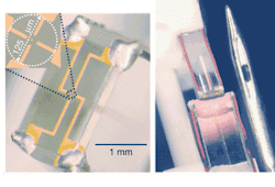
A nematic liquid-crystal (NLC) optical modulator that fits between two single-mode fibers has been fabricated by researchers at Lucent Technologies' Bell Labs (Murray Hill, NJ), the University of Minnesota (Minneapolis, MN), and Brookhaven National Laboratory (Upton, NY). The NLC cell is bounded by the tips of the fibers themselves, in between which are mounted microfabricated electrodes. Filled with the proper NLC material, the modulator operates at polarization-rotating speeds of 1º/µs over an angular range of 1º to 60º.
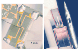
Gold electrodes (left; complete device shown at right with sewing needle for size comparison) are patterned onto two thin glass substrates and a polyimide spin cast onto the substrates to keep the NLC aligned perpendicular to the substrate surfaces. Glass spacer rods 5.5-µm thick create a small gap between the substrates, which is filled at 70ºC with a NLC in isotropic phase, then cooled to room temperature. An electric field between the electrodes temporarily reorients the NLC parallel to the substrates for modulation. A pulsed driving scheme decreases the switching time by a factor of 50 over other methods. The device could find use in polarization analysis and control systems. Contact John Rogers at [email protected]
LEDs march toward shorter wavelengths
Using aluminum nitride/aluminum gallium nitride (AlN/AlGaN) superlattices to reduce defects, a group at the University of South Carolina (Columbia, SC) is achieving ever-shorter wavelengths and higher output powers for ultraviolet (UV) light-emitting diodes (LEDs). In one report, flip-chip-packaged 325-nm-emitting LEDs on sapphire substrates produced continuous-wave (CW) and pulsed powers of 0.84 and 6.68 mW; CW power increased to 1.5 mW at 10ºC. In another result, a buffer-layer growth process reduced nonradiative recombination in a device, allowing it to achieve a pulsed power of 3 mW at a 278-nm wavelength. The LEDs were fabricated using a pulsed atomic-layer-epitaxy deposition process.
Potentially pushing the wavelength envelope even further, the researchers grew high-quality AlN epilayers and Al0.85Ga0.15N quantum wells (QWs) on sapphire that showed strong room-temperature photoluminescence (PL) at wavelengths of 208 nm for the epilayers and 228 nm for the QWs. These results are in contrast to previous reports of deep-UV photoluminescence at similar wavelengths that required cooling to 77 K. The QWs were undoped; silicon doping should screen the built-in electric field and boost PL intensity. Contact Asif Khan at [email protected].
Normal-incidence x-ray mirrors become practical
All imaging x-ray telescopes lofted into space so far have relied on intricate nested sets of deep hyperboloidal mirrors to reflect and focus x-rays. These mirrors, which rely on the fact that some materials reflect x-ray wavelengths at grazing-incidence angles, are extremely difficult to fabricate and hold in position relative to each other. In addition, the far-from-paraxial geometry induces huge aberrations for off-axis points in the field. To solve these problems, normal incidence thin-film reflection coatings for x-rays—requiring almost atomic-thickness layers—have been pursued for years, with unsatisfying results.
Now, researchers at the Columbia Astrophysics Laboratory (New York, NY), Lawrence Berkeley National Laboratory (Berkeley, CA), and Lawrence Livermore National Laboratory (Livermore, CA) have fabricated normal-incidence x-ray mirrors with coatings that, while still low in reflectance, point the way to practical and simple mirrors to focus x-rays. Made of layers of tungsten and boron carbide (a previously identified multilayer candidate), the normal-incidence coatings have 300 alternating layers with periods of 0.8 to 1.2 nm and reflect 1.3% of 2.4-nm x-rays. Practical for some uses even now, such coatings can be further improved with different materials, more layers, and smaller interface widths. Contact David Windt at [email protected].
Biometric optical sensor finds everyday use
A small optoelectronic fingerprint-reading sensor developed by Atmel (San Jose, CA) is being incorporated into certain models of personal digital assistants (PDAs) manufactured by Hewlett-Packard (Palo Alto, CA). With a 0.4 × 14-mm scanning area and an overall package size of 26.6 × 9.8 × 1.5 mm, the sensor is located at the lower edge of the PDA. The user swipes his or her hand vertically across the sensor, which contains a CMOS (complementary metal-oxide semiconductor) device with a resolution of 500 dpi; software then constructs an image and authenticates or denies the user based on a previously stored template.
The sensor measures the temperature differential between a fingertip's skin ridges and the air caught in the fingerprint valleys. The method results in a clear image even on poor-quality fingerprints, such as ones that are dry or worn with little depth between the peaks and valleys of the fingerprint. The swipe method has the side benefit of self-cleaning the sensor and thus avoiding confusion from previous fingerprints. Contact Martin Squibbs at [email protected].
Laser arrays give flowery results
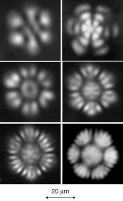
Strongly coupled arrays of vertical-cavity surface-emitting lasers (VCSELs) have produced so-called "light flowers." The six-sided emission patterns resembling flowers are the result of hexagonal arrays of six 10-µm-diameter VCSELs surrounding another in the center, all 1 µm apart. The experimental patterns are formed for injection currents higher than 30 mA and vary depending on injection current and pulse length.
In theoretical modeling, professor Meir Orenstein of the Technion Israel Institute of Technology (Haifa, Israel) and his group confirmed the experimental results and found that the patterns are a combination of Gauss-Laguerre modes. Increased pulse length enhances heat generation, which steepens the waveguide and narrows the beam waist. As injection currents increase from 40 to 80 mA, the number of "petals" increases. The unique emission distributions are due to the effects of thermal lensing when the individual VCSELs change from weak coupling mode to strong array-induced global modes. Whereas the farfield pattern loses its shape for low injection currents, the "flowers" diverge but maintain their shape when the array is strongly coupled. Contact Meir Orenstein at [email protected].
Solgel antireflection film repels water
Researchers at the Chinese Academy of Science (Shanxi, China) are using the solgel process to deposit optical coatings that are both antireflective and highly water repellant. Such coatings will be useful for eyeglasses, windows, vehicle windshields, and more esoteric applications such as optical instrumentation. Deposited by spin-coating a colloidal suspension of silicon dioxide particles in hexamethyldisilazane (HMDS) onto glass substrates, the coatings are then aged for 48 days at room temperature. Low-scattering films were produced with refractive indices ranging from 1.25 to 1.32—ideal for reducing reflection in quarter-wave thicknesses. The lowest monochromatic reflection observed was 0.03%.
More remarkable, however, is the film's water repellence, characterized by the contact angle of a water droplet resting on the film. The closer the contact angle is to 180º, the more spherical is a droplet on the surface (and the smaller is the contact area), and the more water-repellent the film is. Ordinary glass exhibits a contact angle of 8º, while ordinary solgel reaches 38º; in contrast, the HMDS-deposited solgel film showed a contact angle of up to 165º—forcing the droplets into almost-perfect spheres with tiny areas of contact. Contact Yu Han Sun at [email protected].
Gallium nitride-based photodetector
reaches a gain of 1000
A back-illuminated gallium nitride/aluminum gallium nitride (GaN/AlGaN) heterojunction ultraviolet (UV) photodetector developed by scientists at the City College of the City University of New York (New York, NY) and Virginia Commonwealth University (Richmond, VA) has internal gains of up to 1000. Based on metal-semiconductor-metal structures (with gold electrodes) and layers of GaN and Al0.18Ga0.82N, the device has a narrowband spectral response between 343 and 365 nm and a responsivity of up to 133 A/W under weak UV illumination.
The sharp short- and long-wavelength cutoffs defining the spectral response region result from band-to-band absorption of the two semiconductor layers. When chopped at a frequency of 55 Hz, the device shows a responsivity of 1.35 A/W at 359 nm; it is in direct-current mode at 15-V bias and 1.4-nW excitation that the detector reaches its much-higher responsivity. No saturation is observed under voltages up to 15 V. The responsivity is linearly proportional to bias and proportional to the square root of the optical power, explained by trapping and recombination centers. Contact Robert Alfano at [email protected].


