PAUL KARAZUBA
Color imaging and discrimination can be performed in numerous ways. Whether that imaging is based on filter-on-die, filter-on-window, external filter, silicon-depth technology, or one of several other methods, all have the purpose of providing the user with a color image from which information can be disseminated and decisions made. Each method has advantages and disadvantages, and while some of these technologies are more in use than others, each has unique features that allow it to be a viable choice for users.
A CCD/CMOS chip cannot distinguish color without one of these technologies. When a chip operates without any sort of color-separation technology, the chip images and provides information on its target in terms of gray-scale and essentially collects all light within its sensitivity range—for silicon-based chips, usually between about 250 to 1000 nm—without knowing what percentage of that light is within a given spectral range.
Typically, overall color is determined using a combination of three colors—red (600 to 650 nm), green (500 to 550 nm), and blue (400 to 450 nm) that are filtered by one of the aforementioned methods. Many combinations of filter bandwidths are available but only these three colors will be discussed here for the sake of clarity. Common color data from each pixel is collected independently and read out through separate channels unique to that color. The sensor electronics, programmed to recognize which color (red, green, blue) is passing through a specific channel, measure the varying intensity of those channels and combine the data to form what becomes a color image to the user. The actual color-data combination process then becomes very similar to painting, in which a specific quantity of red paint (data), combined with specific quantities of green and blue paint (data), form the overall color represented by that specific combination.
Filter-on-die color separation
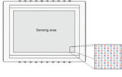
The filter-on-die color-separating technique is based on actually laying down color-filter material directly onto the silicon surface of the CCD/CMOS chip. The filter pattern changes, depending on the sensor and the sensor architecture. The most popular pattern on an area sensor is a mosaic filter (also know as a "Bayer"), which is similar in appearance to a checkerboard. Each individual pixel within the sensor is covered by a single wavelength filter that allows only specific wavelengths to pass. Neighboring pixels are then covered with a different wavelength filter (see Fig. 1).
This method offers the advantage of a relatively easy process for filter construction and manufacture. In addition, all colors are imaged on the same chip and only one channel of sensor electronics is needed. However, the method only allows one-third (or one-quarter, depending on filter architecture) of available pixels to image a specific color. In addition, once the filter is implanted on the sensor die it cannot be changed to suit a different need, and color filters tend to white-bleach after extended use, eventually becoming unusable.
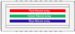
On-line scan devices using "filter-on-die"' technology can be implemented on the sensor in two ways. The first is very similar to the mosaic area-scan filter, in which each successive pixel has a different filter element implanted on top. The second method involves tri-linear devices. In a tri-linear CCD, the actual sensor package contains three parallel CCD/CMOS linear arrays, placed together at distance equal to a multiple of the pixel size. In this method, each linear array is individually filtered to receive only one color (see Fig. 2).The mosaic linear-filter method offers the same advantages and disadvantages as the mosaic area-filter method, plus some unique advantages. With tri-linear, there are three linear arrays, each imaging a separate color, so it is not necessary to sacrifice resolution, like with the mosaic method, because every point in the field of view is being imaged with a red, blue, and green sensor elements. On the other hand, since the three linear arrays are located at a physical distance from each other, users have historically had to write custom software algorithms in which the speed of their target has to be combined with the linear-array separation distance and sensor speed to recombine that image. PerkinElmer has developed and implemented a patent-pending technology that allows this calculation to be performed automatically in the camera head, removing the development time and resources formerly placed on the user.
Other color separation methods
The filter-on-window method involves a single or group of filter strips to be applied to the protective window of a chip. This method is usually implemented to allow customization of sensors based on user needs. The actual filter architecture is similar to the filter-on-die method, in which either each individual pixel is filtered, or a group of pixels are filtered together. This method allows each sensor to be customized based on filters. Its disadvantages include primarily problems associated with the alignment of the filter vs. the sensor die, as well as the filter bleaching mentioned earlier.
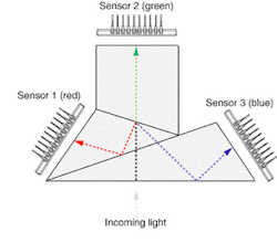
Color imaging can also be performed using an external filter, in which three individual sensors are mounted with a beam-splitting filter placed in front. The filter has an input side, as well as three outputs (depending on the filter). The light passes through the front of the filter and is internally separated into wavelength groups (see Fig. 3). Those groups are passed to individual sensors, which image only that color.The use of an external filter eliminates the issue of color bleaching. Also, the filter can be replaced, which allows for easy customization of the product. The issue of spatial differences with tri-linear devices is also solved, as the three linear sensors are imaging the same target at the same time. However, using three sensors, each with its own set of electronics, is typically space- and cost-intensive. These cameras also can be subject to misalignment due to poor manufacturing or extreme vibration, and often require expensive optics to operate.
Recently, Foveon (Santa Clara, CA), demonstrated a process in which sensors are designed using the penetration depth of wavelengths to filter color. Basically, the longer the wavelength, the further into the silicon surface the light will penetrate. By actually layering pixels on top of one another, these sensors can distinguish the color of the light received based on which layer of pixels received the light. What results is essentially three times the number of pixels within the same sensor area.
Current color-filtering methods are still viable and will continue to dominate for years to come. While there are many different products available using every one of these technologies, new technologies will inevitably be integrated into these types of applications, allowing users even more choices when it comes to their color-imaging requirements.
PAUL KARAZUBA is the product manager for the PerkinElmer Optoelectronics CCD group, 2175 Mission College Blvd., Santa Clara, CA 95054; e-mail: [email protected].


