KEITH ANDERSON and IAN BETTY
External modulators are used in high-performance fiberoptic transmission systems to avoid laser chirp (transient changes in the transmission wavelength), ringing, and limited extinction ratio. Further benefits stemming from modulators are possible if chirp can be carefully controlled.
Because of fundamental physical principles, optical data transmitted at high rates has a significant spectral spread. Acted on by the dispersion of an optical fiber, the spectral spread becomes a spread in the time domain. For example, 10.7-Gbit/s non-return-to-zero (NRZ) data has a power spread across 5 GHz of spectrum (the Fourier transform of the data). After transmission over 100 km of standard fiber with a dispersion of 17 ps/nm-km, that 5-GHz frequency spread develops into a time-domain smear of about 70 ps—bad news when the data period is 93 ps.
The correct pulse chirp can combat this problem. Imposing some red (frequency reduction) chirp on the leading edge of each pulse and some blue (frequency increase) chirp on the trailing edge tends to compress the pulse as it travels along standard fiber, enabling well-engineered 10.7-Gbit/s links to extend beyond 100 km (see Fig. 1).
The preferred external-modulator setup enables accurate control of chirp using an interferometric Mach-Zehnder (MZ) waveguide configuration. An MZ works by splitting the source light into two paths (arms) and phase-shifting one path relative to the other; under recombination, the light is directed to either the output fiber, a '1,' or to an optical dump port, a '0.' The relative phase shift between a '1' and a '0' must be 180∞, but the contribution from each arm to the output can be selected in many different ways to produce the correct sign and amount of net chirp. Because MZ modulators are primarily interferometric and absorb little light, they can be used to modulate high-power signals without problems.
Stark effect
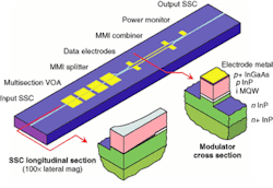
In our indium phosphide (InP) MZ modulator chip, the continuous-wave (CW) input from the laser source enters the chip via an optical-mode spot-size converter (SSC), passes through an absorptive-style variable optical attenuator (VOA), and is then divided between the two arms of the modulator using a multimode interference splitter (see Fig. 2).1, 2 The optical signal in one modulator arm is phase-shifted relative to the other by an external drive voltage applied to the electrode on each arm. The signals are then recombined via another multimode interference combiner into either a waveguide containing an optical power detector, or an output waveguide containing a second optical-mode spot-size converter.A strongly guiding ridge is deeply etched into p-i-n layers to form the modulator waveguide. The thin intrinsic region of the p-i-n contains a multiple-quantum-well (MQW) modulator core with 20 95-Å indium gallium arsenide phosphide (InGaAsP) wells and 21 80-Å InGaAsP barriers. The guided mode is highly confined to the MQW core, enabling good overlap efficiency with the large electric field that can be created across this thin intrinsic region.
In the MZ arms, the quantum-confined Stark effect (QCSE) is used to convert the applied electrode field into an effective refractive index change and hence an optical phase shift to the propagating mode.3, 4 For a given electrode voltage, the phase shift induced by the QCSE depends on the relative offset between the modulator operating wavelength and the peak excitonic wavelength resonance in the quantum-well material. For a relative offset of approximately 135 nm, a large phase shift can be achieved with only a small increase in material absorption. Compared to other MZ modulator designs using the linear electro-optic effect, the QCSE enables an MZ modulator with short, high-bandwidth lumped-element electrodes that require differential electrical drive signals of less than 3-V peak to peak.
Spot-size converters
The narrow ridge and thin guide core enable short chips with low drive voltage, but make direct optical coupling challenging. Integrated spot-size converters (SSC), each only 0.5 mm long, address that problem. The SSC cores are butt-joined to the MZ waveguide by a precision dry-etch and metal-organic chemical-vapor-deposition selective-area growth (SAG) process. The thickness of the passive core tapers from 0.2 µm at the butt joint down to 0.05 µm at the face—the optical mode is less confined and expands as the layer pinches. Simultaneously, the SSC waveguide ridge flares laterally from 2 µm at the butt joint to 4.5 µm at the facet. The design results in an adiabatic transition from the MZ waveguide mode to a chip facet mode with a symmetric full-width-half-maximum 18° × 18° far-field pattern that can be coupled to efficiently.
Other InP-based features
Other features of the InP-based modulator are QCSE modulation and SAG, which combine to enable high efficiency chips only 3 mm long. This results in a low cost per chip because many thousands can be fabricated on a 3-in. InP wafer using methods similar to laser production. A further unique advantage of the InP system is that the device operates close enough to the quantum-well material-absorption-band edge to enable the monolithic integration of simple variable-optical-attenuator (VOA) structures and power-monitor detectors onto the chip with little impact on device cost or other performance metrics. A version with a monolithically integrated distributed-feedback (DFB) laser has been demonstrated.5 Integrated semiconductor optical amplifiers offer another possible extension of the InP capability.
Copackaging
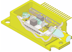
The small modulator-chip size invites copackaging with a CW laser. Bookham Technology, through its acquisition of Nortel Networks, has been producing such copackaged sources for OC-192 and 10.7-Gbit/s transmission since 1995. The latest version is optimized for transponder and dense-card applications (see Fig. 3).The MZ response has some temperature dependence, but because the chips are small and dissipate little power, mounting them on the same thermoelectric cooler (TEC) as the laser is practical.6 If that TEC is used to thermally tune the laser, for example across an 8 × 50-GHz set of ITU-grid wavelengths, the temperature dependence of the modulator and the laser differ enough to require different MZ drive levels at each tuning temperature. Otherwise, the performance is similar across that band.
As in all high-performance DFB-based transmission sources, an optical isolator is needed to protect the laser from external feedback. Placing that isolator between the laser and modulator acts as a safeguard against reflections from the MZ output facet which, being modulated, are particularly problematic. Lenses are therefore required, first to collimate the laser output and subsequently to launch it into the MZ-coupling waveguide. Those two have high numerical apertures and must mount very stably. A relatively weak lens, in this case mounted on the optical isolator, is aligned last to steer the beam slightly and optimize the coupling into the MZ. All the optics mount on a single ceramic platform which in turn mounts on a TEC.
Wavelength-monitoring optics are fixed on the laser subcarrier, and the radio-frequency-termination components needed by the differential 10.7-Gbit/s data signals are incorporated into the MZ carrier. Both the VOA and output monitor are integrated into the modulator chip and therefore do not show as discernable components. All of the electrical connections, including the controlled impedance differential data, are arranged along a single side of the 8.1-mm-high industry-standard-footprint package.
Monolithic laser/MZ integration would appear to be the crowning advantage of InP. Hybrid copackaging, however, delivers the same end benefit and offers significant developmental and logistical advantages. Managing demand for dense-wavelength-division-multiplexing wavelengths has been much easier with separate lasers; the MZ is relatively "colorblind." We have also been able to use the lasers, and indeed the same chip-on-carrier subsystem, in other products such as CW lasers and copackaged gallium arsenide-based MZ transmitters. Discrete laser and MZ chips have been easier to improve independently, both for technical reasons and inventory management across the ITU grid during commercial introduction. Improvement examples are brighter lasers (with up to +7-dBm modulated launched power), MZ chirp flavors (now negative, selectable-negative or positive, and zero), and MZ-chip features (the VOA, power monitor, and SSCs).
REFERENCES
- C. Rolland et al., Elec. Lett. - IEE 29, (1993).
- J. Cartledge et al., IEEE Phot. Tech. Lett. 6, 282 (1994).
- J. Yu et al., IEEE Phot. Tech. Lett. 8, 1018 (1996).
- W. Bardyszewski et al., J. Appl. Phys 80, 1136 (1996).
- D. Adams et al., Elec. Lett. - IEE 32, 485 (1996).
- M. Allard et al., Temperature Determination in Optoelectronic Waveguide Modulators, JLT 18, 813 (2000).
Keith Anderson is the designer of copackaged laser/modulator transmit modules and Ian Betty is the designer of InP MZ chips at Bookham Technology, PO Box 3511 Station C, Ottawa, ON, K1Y4H7, Canada; e-mail: [email protected] and [email protected].


