Optics have high post-coating flatness
Many optics manufacturers offer optics with a flatness of λ/10 or better. Flatness specifications often only apply to the substrate prior to coating, however, and mechanical stress in a thin-film coating can warp a component substantially out of shape. Environmental factors, such as temperature and humidity, also affect part shape. For these reasons, performance specifications for off-the-shelf optics often fail to tell the whole story.
Stress and flatness
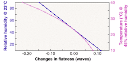
Most optical thin films are deposited at high temperature, and mechanical stress is introduced into a coating when the part subsequently cools (see Fig. 1). The stress in each coating layer can be either compressive or tensile, depending upon the materials used and the exact deposition process parameters. In addition, water absorption due to atmospheric humidity can later cause additional time-varying changes in internal thin-film stress. The net result of all these effects is that an optic originally specified at λ/20 might end up with a surface accuracy of only λ/4 in actual use (see Fig. 2).
Water-absorption effects are most pronounced in porous thin films. Various coating densification methods, such as ion-assisted deposition or sputtering deliver more environmentally stable films. These dense films contain inherently more stress to begin with, however, and are thus more likely to warp a substrate out of its original shape. Furthermore, dense films often exhibit lower damage-threshold characteristics than porous coatings. Thus, for high-flatness and high-damage-threshold optics, porous films remain the predominant choice; as a result, the issue of humidity-related stress must be addressed, and conditions in the final-use environment must be known in order to accurately predict component performance.
The total amount of product distortion caused by coating stress is primarily determined by its aspect ratio, which is the ratio of the part's longest dimension to its thickness. It has been fairly standard in the optics industry to use a substrate aspect ratio of 6:1 or less when producing λ/10 or better optics. But based on our experience at Alpine Research Optics, we have found that it is safer to use an aspect ratio of 5:1 or less to consistently produce high-flatness optics in volume. This is because part deformation increases with the square of the aspect ratio; thus, going from just 6:1 to 5:1 results in a nearly 30% improvement in distortion resistance. Substrate material also plays a role because various materials have different stiffness characteristics.
The substrate-fabrication process also can introduce stress into the bulk material, even before coating. This is because operations such as milling, grinding, and polishing apply pressure to the substrate and cause subsurface damage. It is most effective to relieve internal stress before final polishing so that the part doesn't "spring," or continue to change shape, during final figuring. Stress relief can be accomplished by process steps such as polishing part edges or polishing the second surface of an optic, instead of just producing a fine grind (the latter only applies to optics that operate in a first-surface mode, such as high reflectors). Parts can also be temperature-cycled to pre-anneal them before final processing.
Understanding specifications
Part flatness can be specified in a variety of ways. The first step in obtaining flat optics is to fully understand how a manufacturer defines and specifies flatness. Any discussions with that manufacturer must be conducted in a common language to avoid misunderstandings, and customer-produced drawings and specifications should clearly state what definitions are being used and how they are applied.
One simple way of specifying flatness is peak-to-valley. This is the height difference between the highest and lowest parts on the surface of the piece. Another definition of flatness divides the specification into two separate components: power and irregularity. Power is the spherical deviation in overall part shape from the desired surface—a perfect flat plane in the case of a flat optic. Irregularity refers to small-scale surface imperfections.
The power and irregularity definition is particularly useful when addressing post-coating flatness issues. This is because the coating process and subsequent environmentally induced changes most commonly distort an optic in a way that creates either spherical or cylindrical power. Conversely, small-scale irregularities in an optical surface are there from the outset and generally don't vary because of coating and post-coating factors. Thus, the irregularity specification provides a clear measure of the best a part will ever perform under any circumstances, while the power number gives an indication of the magnitude of post-coating-related effects.
In contrast, a peak-to-valley flatness measurement only provides a broad description of what is happening to component shape without clarifying which types of imperfection are dominating the result. Furthermore, the absolute value of the power added to irregularity always produces a number that is greater than or equal to the peak-to-valley result, making it a more conservative measure of part flatness.
When specifying parts, it is important to remember that the actual effect on wavefront depends on whether a part is reflective or transmissive. In the case of a reflector, the wavefront is distorted by twice the value of the surface specification at normal incidence. A transmissive optic only distorts the wavefront by roughly half the surface specification; the actual value depends on the refractive index and angle of incidence.
Questions should be asked of any prospective vendor of high-flatness optics. First, it should be established whether flatness or transmitted-wavefront specifications are meant to apply just to the substrate, or to the finished and coated part. Also, it is more useful to specify optics in terms of actual wavefront distortion rather than flatness. This takes into account all the use-dependent factors.
It is also essential to ask how specifications are measured. Ideally, flatness and wavefront distortion should be measured with an interferometer. The buyer of high-performance optics should feel entitled to an interferogram of that very part, not a representative sample; however, one should expect to pay for this service.
It is necessary to ascertain the conditions under which the testing is performed. Are parts measured under the intended temperature and humidity use conditions? If not, can the vendor reliably calculate the performance shift between the measured and end-use conditions? In some cases, the substrates have been fabricated and measured by another manufacturer—the vendor thus loses control over the precise testing conditions.
We purchased three 2-in.-diameter optics from three major catalog suppliers. The results of interferometric testing highlight the need for obtaining proof of performance (see table). In the worst case, an optic specified as λ/10 had an actual surface figure of only λ/5.
Part of the burden for achieving the required part performance rests with the user. Specifically, it is necessary to accurately specify the nominal operating temperature and humidity, as well as the total possible variation in both these parameters. Understand, however, that the broader the operating range, the more expensive the part.
Achieving high post-coating flatness
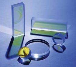
There are a number of fabrication techniques targeted at achieving high post-coating flatness (see photo, p. S9). One approach involves prefiguring. This is purposefully polishing a slight curvature on a substrate with the intention of having the coating stress distort the optic back into flatness. Unfortunately, this is a somewhat empirical process and it is also difficult to reliably produce the very slight curvatures required. The result is that production yields using this approach are low.
Another technique, useful for first-surface reflectors, is backside coating. Specifically, a single-layer coating, typically of silicon dioxide, is placed on the second surface of the optic. The purpose is to balance and null out the overall mechanical stress on the part. This approach is particularly popular with scanner mirrors, which often have a poor aspect ratio. Once again, the major drawback of this method is its unpredictability, making it problematic for use in volume manufacturing.
At Alpine Research Optics, we have developed an approach for reliably achieving high post-coating flatness based on our experience in producing demanding optics for the Lawrence Livermore National Ignition Facility project in Livermore, CA. This process begins with the production of a substrate possessing high flatness in terms of both power and irregularity. Substrate flatness is achieved by careful application of relatively traditional optical-fabrication techniques. A multilayer-dielectric thin film is then applied that is specifically optimized to introduce minimal distortion to the part; the coating has a combination of materials with both tensile and compressive characteristics.
In addition to minimizing overall stress, the design is optimized to produce the required damage threshold, mechanical durability, and spectral performance. Most important, the relationship between temperature/humidity and coating stress has been successfully characterized. Understanding how coating stress changes between production conditions and the final operating environment has enabled the design and consistent production of optics that meet specification in actual use.
DAVID KEMP is eastern regional sales manager and WAYNE PANTLEY is sales manager and marketing manager at Alpine Research Optics, 3180 Sterling Circle, Boulder, CO 80301; e-mail: [email protected].


