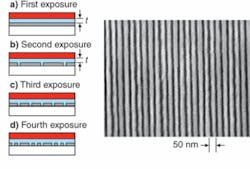
Although still not capable of producing the complex, nonperiodic structures necessary for most integrated-circuit (IC) designs, interference lithography has been used to successfully fabricate grating structures with a period of 50 nm.1 The gratings were patterned at the Massachusetts Institute of Technology (MIT; Cambridge, MA) Space Nanotechnology Laboratory.
Semiconductor ICs are currently fabricated using immersion lithography and/or nanoimprint lithography (NIL) and other techniques to achieve fine feature sizes; however, lithography techniques are also used for the fabrication of high-density grating structures. “Nanoscale periodic patterns, while having myriad scientific and commercial applications, are notoriously difficult to produce with the high throughput and tight tolerances necessary to achieve nanodevices with low cost and high yield,” says Mark Schattenburg, senior research scientist at MIT says.
Schattenburg notes that commercial applications of nanoscale periodic patterns include CMOS circuits, patterned nanomagnetic media for disk drives, nanophotonic/nanobio devices, and solar cells. “Multilevel interference lithography has the potential to enable commercialization of a host of new nanotechnology inventions, many of which have languished in laboratories due to the lack of a viable manufacturing paradigm,” he says. “Our efforts now are focused on simplifying the fabrication process and further tightening process controls into the subnanometer range,” he says.
Spatial-frequency multiplication
Interference lithography offers large exposure areas and high spatial-phase coherence compared to other methodsan interference pattern between one or more coherent light beams is recorded in an optical material. Ordinarily, however, the spatial resolution (smallest attainable period of the features) is limited by the wavelength (λ) of the light source used and the refractive index (n) of the recording material according to λ/2n. The MIT researchers refined this basic method by using an alternative spatial-frequency-multiplication process that uses multiple exposures through grating patterns aligned with high accuracy, overcoming the wavelength-limited resolution problem.
To fabricate the 50-nm-period gratings, a silicon nitride reference grating with a period (p) of 200 nm is patterned in the outer region of a substrate using interference lithography and a source with a 351.1 nm wavelength, serving as a fiducial pattern for subsequent steps in the process. Photoresist and an antireflection coating are then spun on top of this reference grating. The first grating level, also with p = 200 nm, is then aligned and exposed at a relative phase offset to the reference grating, with linewidth w. The grating pattern is then transferred into the nitride layer and the process is repeated, with the second grating level exposed at an additional π-phase offset. After pattern transfer, the nitride grating has a period of p/2 = 100 nm. This process can then be repeated to further reduce the period, depending on the duty cycle w/p of each grating level.
For accurate overlay alignment, the phase of the reference grating is mapped prior to the lithography process so that each grating level can be exposed with the proper phase shift. To optimize the phase signals, the reference grating is designed such that the diffracted orders are balanced in intensity. The precise grating alignment is accomplished using the MIT nanoruler—a scanning-beam-interference lithography technology developed previously at MIT.2
To achieve high-spatial-frequency multiplication factors for the process, a high-duty-cycle grating period with nanometer-level repeatability is needed for each grating level. Oxygen plasma etching is used to control the grating linewidth, and an image-reversal process is used to transfer the thin-line pattern into a high-duty-cycle pattern. With the use of grating patterns with an approximate 0.88 duty cycle, fourfold spatial-frequency multiplication can be achieved by overlaying four phase-shifted grating levels.
The interim result from a spatial-frequency-doubled process patterned twice with a 200-nm-period grating at 351.1 nm is a 100-nm-period grating with a phase overlay accuracy and linewidth variation both better than 5 nm over a 35 × 20 mm area. The fourfold or four-exposure process produces 50-nm-period gratings with feature sizes down to approximately 25 nm.
REFERENCES
1. C.-H. Chang et al., Optics Lett. 33(14) 1572 (July 15, 2008).
2. R.K. Heilmann et al., Nanotechnology 15, S504 (2004).

Gail Overton | Senior Editor (2004-2020)
Gail has more than 30 years of engineering, marketing, product management, and editorial experience in the photonics and optical communications industry. Before joining the staff at Laser Focus World in 2004, she held many product management and product marketing roles in the fiber-optics industry, most notably at Hughes (El Segundo, CA), GTE Labs (Waltham, MA), Corning (Corning, NY), Photon Kinetics (Beaverton, OR), and Newport Corporation (Irvine, CA). During her marketing career, Gail published articles in WDM Solutions and Sensors magazine and traveled internationally to conduct product and sales training. Gail received her BS degree in physics, with an emphasis in optics, from San Diego State University in San Diego, CA in May 1986.
