Holographic lithography enables complicated 3-D photonic crystals

Feb. 1, 2008
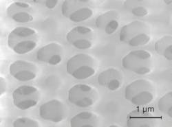
To develop novel optical microstructures with potential in photonic, microfluidic, biomedical, and micromechanical applications, scientists at the State Key Laboratory of Optoelectronic Materials and Technologies at Zhongshan University (Guangzhou, China) have created a technique to fabricate complicated three-dimensional (3-D) photonic crystals using single-exposure holographic laser lithography.

To develop novel optical microstructures with potential in photonic, microfluidic, biomedical, and micromechanical applications, scientists at the State Key Laboratory of Optoelectronic Materials and Technologies at Zhongshan University (Guangzhou, China) have created a technique to fabricate complicated three-dimensional (3-D) photonic crystals using single-exposure holographic laser lithography. Seven linearly polarized laser beams in two configurations were used to create an interference pattern deposited on a photoresist film 40 µm thick. After polymerization, development, and drying, the 3-D pattern measured 25 µm, and consisted of a hexagon motif (a kagome lattice) on the surface with a chainlike lattice on the cleavage plane.

Transmission through three different layers of the hexagonal microstructure creates a diffraction pattern resembling fireworks. Transmission spectra reveal a dropoff below about 1700 nm, with a partial photonic bandgap between 1.9 and 2.25 µm. The next step in the plan, according to team member He-Zhou Wang, is to fabricate new photonic crystals with wide bandgaps in the visible. Such structures will have novel properties that can be exploited much like those of well-known electronic crystals. Contact He-Zhou Wang at [email protected].
Sponsored Recommendations

Advancing Neuroscience Using High-Precision 3D Printing

March 7, 2025
Learn how Cold Spring Harbor Laboratory Used High-Precision 3D Printing to Advance Neuroscience Research using 3D Printed Optical Drives.

From Prototyping to Production: How High-Precision 3D Printing is Reinventing Electronics Manufacturing

March 7, 2025
Learn how micro 3D printing is enabling miniaturization. As products get smaller the challenge to manufacture small parts increases.

Sputtered Thin-film Coatings

Feb. 27, 2025
Optical thin-film coatings can be deposited by a variety of methods. Learn about 2 traditional methods and a deposition process called sputtering.

What are Notch Filters?

Feb. 27, 2025
Notch filters are ideal for applications that require nearly complete rejection of a laser line while passing as much non-laser light as possible.

Voice your opinion!

To join the conversation, and become an exclusive member of Laser Focus World, create an account today!