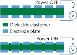
Liquid-based variable-focus (varifocal) lenses, from miniature to large, have been thoroughly researched and have made their way into the commercial market. In contrast, varifocal lenses based on flexible solids are few and far between, but researchers at the University of Tokyo (Tokyo, Japan) have designed and fabricated a robust varifocal microlens array that operates by applying a voltage across a flexible transparent dielectric elastomer to force the elastomer into an array of holes in the metal electrodes, changing the surface of the elastomer from flat to biconvex. The process works via an effective Maxwell electrostatic stress, experienced by the elastomer as a compressive stress. The curvature of the microlenses increases in proportion to the applied voltage.
The researchers first modeled a 3 × 3 microlens array with 1.5 mm apertures and polyacrylate as the polymer material using multiphysics simulation software from COMSOL (Burlington, MA), which confirmed that a lens-shaped surface would result from an applied voltage. They then fabricated a 9 × 9 microlens array with 1-mm-diameter apertures and a 1-mm-thick acrylic as the elastomer (the material, VHB 4910 by 3M, was originally designed as a double-sided adhesive tape). To characterize the device, voltage was applied in steps of 0.5 up to 5 kV and a tilted test target was imaged through the microlens array (testing each of the elastomer microlenses one by one with an occluder that blocked all but one lens). Based on the shift in focus of the test target, the focal length of the microlenses at the highest voltage was calculated to be 950 nm (and a zero voltage was infinity). In addition, a 1951 USAF resolution target was imaged at good quality through one of the microlenses alone. Reference: L. Wang et al., Opt. Express (2017); https://doi.org/10.1364/oe.25.031708.

John Wallace | Senior Technical Editor (1998-2022)
John Wallace was with Laser Focus World for nearly 25 years, retiring in late June 2022. He obtained a bachelor's degree in mechanical engineering and physics at Rutgers University and a master's in optical engineering at the University of Rochester. Before becoming an editor, John worked as an engineer at RCA, Exxon, Eastman Kodak, and GCA Corporation.
