All-calcium fluoride system uses 157-nm light
JAMES WEBB
Three years ago, the use of 157-nm radiation for exposing and printing integrated-circuit (IC) chips was not even on the International Sematech National Technology Roadmap for Semiconductors.1 Today, it is anticipated that 157-nm lithography will supersede 248- and 193-nm lithographic processes as they reach their limits. Current projections are that 157-nm optical systems will be used in production by 2005 for 100-nm features and smaller. Numerous research-and-development efforts are under way worldwide to develop the new technologies needed to make this next generation of ICs.
In one of these efforts, a 157-nm catadioptric system has been designed, fabricated, and tested at Tropel Corp. (Fairport, NY). The intended use of this optical system is to support photoresist-process development for printing 130-nm features and smaller. Transmissive vacuum-ultraviolet (VUV) photomask (reticle) technology and contamination-free atmospheric-nitrogen-purging environments for both the reticle and wafer planes were among the biggest challenges for wafer-stepper manufacturers to have in place before this optical system could be used.
Optical design
Tropel previously has developed an in-line, on-axis catadioptric optical system containing only fused silica (SiO2) as an optical material. Designed for operation with a free-running non-line-narrowed, 193-nm excimer-laser source, the system has been used for the development of 193-nm resist technology (see cm Feb. 1997, p. 75). The optical system consisted of a beam-delivery module, an illuminator, and a projection lens. Sixteen such systems have been installed worldwide in wafer-stepper cameras supporting 193-nm development processes.
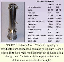
With a few modifications, this same catadioptric design form is now being used at 157 nm (see Fig. 1). Conventional SiO2 does not transmit sufficiently at 157 nm; at this wavelength calcium fluoride (CaF2) is the refractive material of choice, as it has a transmission of greater than 99%/cm. Because the index of refraction of SiO2 at 193 nm is nearly the same as the index of refraction of CaF2 at 157 nm (both are approximately equal to 1.56), the optical-design changes to the catadioptric system were minimal. At VUV wavelengths, the optical path must be purged (usually using nitrogen as the purge gas); thus it became necessary to add several plane-parallel plates to the design to establish boundary controls for isolating the nitrogen-purging chambers.
The free-running spectrum of the 157-nm fluorine excimer laser contains two lines separated by 100 pm, each having a full-width-at-half-maximum bandwidth less than 1 pm wide. Chromatic correction over the bandwidth is achieved in the catadioptric design form by putting most of the optical power in the reflecting surfaces, making the sum of the power of the refractive components nearly equal to zero.
The system contains five main chambers for nitrogen purging of the optical train. The beam-delivery, illuminator, and projection-lens modules have purge fittings to isolate and provide separate controls. In the illuminator, a removable aperture drawer is provided that is conjugate to the pupil of the projection lens. This allows insertion of different plates that permit variation of illumination conditions. The reticle is frequently changed during stepper operation, with the frequency depending on the types of wafer features that are being exposed. Plane-parallel window barriers made of CaF2 are placed close to the reticle so that the purging volume around it can be minimized. Separate purge control is necessary for the space between the last optical surface of the projection lens and the wafer plane. Both the reticle-chamber and wafer-plane purging areas are controlled by systems independent of the projection lens. (They are part of the stepper camera.)
New approaches fit needs
Significant new technologies were developed to meet the needs of this new lithographic system. Calcium fluoride material characterization, deterministic polishing processes, coating technology, metal finishing, purging technology, and test methodology were all critical developments for this optical system.
Special requirements and processes are needed for 157-nm lithography-grade CaF2. Single-crystal material was selected oriented in the 111 plane, with better than 1 x 10⁻⁶ refractive-index homogeneity, birefringence below 2 nm/cm, bulk transmission greater than 99%/cm, and purity high enough to be able to withstand greater than 1-mJ/cm2 power density within the projection lens. Calcium fluoride material selected for the beam-delivery and illumination systems must withstand greater than 3-mJ/cm2 power density and have a bulk transmission greater than 99%/cm, although with relaxed homogeneity and birefringence specifications.
The differential hardness of the CaF2 material causes asymmetric surface-finishing errors when polishing steeply curved spherical surfaces. This is a result of the cubic structure of CaF2 crystals. When the material is oriented in the <111> plane, a three-point surface error is created when it is conventionally polished. This error is much larger than the demanding surface specifications required for high-resolution lithographic imaging. To solve this problem, deterministic polishing methods were developed that minimize residual surface errors on polished CaF2 components. This capability allows surfaces to be polished spherically to better than 2 nm rms. Resulting surface roughness errors are typically better than 5 Å rms.
Optical coatings must last
Coating technology had to be developed for robust high-reflectivity mirrors, beamsplitters, and antireflection coatings. The biggest challenge was to find the right combination of process steps and materials that provide high-efficiency coatings while ensuring that the combination does not degrade over time at the fluence levels required.
Before high-efficiency 157-nm coatings could be designed, special metrology had to be obtained to measure thin-film optical properties of transmissive materials. Tropel received the first VUV ellipsometer made by J. A. Woolham Co. (Lincoln, NE) that operates at wavelengths down to 145 nm. This instrument was made available through the support of International Sematech, while Massachusetts Institute of Technology Lincoln Laboratory (Lincoln Lab; Lexington, MA) provided early support of material and spectral analysis. Lincoln Lab also performed coating life tests using 157-nm excimer-laser sources.
Module efficiency
Although the catadioptric optical design is very similar to the 193-nm system, it was necessary to make significant modifications to the mechanical assemblies. These changes were mostly driven by the need to have vacuum-like sealed assemblies, but purged slightly above atmospheric pressure with ultrahigh-purity nitrogen, because 157-nm radiation is absorbed primarily by residual amounts of water vapor, oxygen, and hydrocarbon contaminants at the parts-per-million level.
To achieve sealing, metal-finishing processes had to be modified. All mechanical surfaces are finished to minimize surface roughness and then sealed with nickel plating to eliminate contaminants that would outgas and shorten the lifetime of the optical system. Metal parts also are baked at an elevated temperature following general high-vacuum practice. Assembled components with connecting mechanical surfaces are made precise enough that they provide a barrier to the outside atmosphere and at the same time allow nitrogen to purge continuously throughout the internal assemblies. Optomechanical bonding materials used for mounting and aligning components have been selected that do not outgas.
Boiled-off liquid nitrogen is delivered in baked stainless-steel tubing through point-of-use filters that further prevent contaminants from entering each module. Oxygen and water-vapor levels inside each module are reduced to the parts-per-million level before 157-nm radiation is transmitted by purging the modules with nitrogen for several hours. With oxygen and water-vapor levels stable at the parts-per-million level, the transmission of each module is measured.
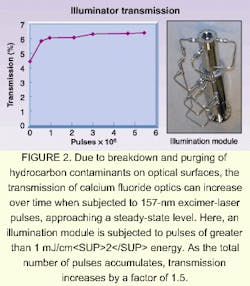
As has been predicted by Lincoln Lab researchers, the transmission increases with the number of laser pulses as trace hydrocarbon contaminants on optical surfaces are broken down and carried away by the nitrogen flow (see Fig. 2). Hydrocarbon levels are reduced to parts-per-billion levels after adsorbed layers on optical components are "laser cleaned" in this way.The beam-delivery system contains two antireflection (AR) coatings and two turning mirrors and reaches a transmission of 35%. The illuminator module has refractive components that include 14 AR coatings, one hollow integrating rod, and two diffusers. Total transmission of this module measured 6.5%. The projection lens has six refractive components that include 11 AR coatings, one beamsplitter, and one high-reflective mirror. Transmission of the projection-lens module measured 4%.
Wavefront testing at a longer wavelength
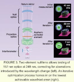
Tropel uses off-wavelength transmitted-wavefront testing as part of a closed-loop optimization process to provide nearly perfect imagery of the projection optics (see Fig. 3). A 248-nm Twyman-Green interferometric null-test method developed for the 193-nm objectives was modified to work at the 157-nm wavelength. A more-complicated two-element null group is attached to the projection-optics assembly when testing for wavefront errors. This corrective null compensates for aberrations caused when measurements of the objective are made at a 248-nm wavelength. The aspheric departure of the corrector plate that is part of the objective design is used as a variable to optimize residual symmetric and asymmetric wavefront errors. Initial measurements of the projection lens are used as optimization targets for minor adjustments to the aspheric plate. Several objectives have been completed, each having wavefront errors of less than 7 nm rms.After the projection-lens assemblies are completed, final wavefront measurements are fed into a lithographic-modeling program to determine if the optical systems will print 130-nm imagery over the 300-nm depth of focus and 2.1-mm-diameter image field. This image modeling includes aerial-image analysis of periodic and isolated structures. Model results show aerial-image features with critical dimensions that vary less than 15 nm over the entire image field.
Encouraging results have been obtained from this broadband catadioptric system. Recent installation into a wafer stepper using a fluorine excimer-laser light source has allowed exposures to be made at 157 nm for determining resolution. Future work will demonstrate that, when combined with new photoresist processes, CaF2 optical systems operating at a 157-nm exposure wavelength can extend optical lithography to well below 100-nm critical dimensions.
REFERENCE
- National Technology Roadmap for Semiconductors, International Sematech (Austin, TX; www.itrs.net/ntrs/publntrs.nsf).
James Webb is a technical director and the optical design manager at Tropel Corp., 60 O'Connor Rd., Fairport, NY 14450; e-mail: [email protected].


