HOLOGRAPHIC LITHOGRAPHY: Interference builds 3-D photonic crystals

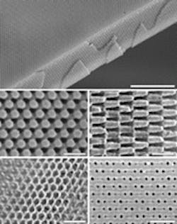
Three-dimensional (3-D) photonic crystals intended for the visible and near-infrared regions are far more difficult to fabricate than their two-dimensional analogs, which are made by techniques that include conventional and holographic lithography. Various methods have been developed to make 3-D photonic crystals, including self-assembly of polymer spheres (see Laser Focus World, April 1999, p. 26) and stacking of lithographically patterned layers (see Laser Focus World, Dec. 1999, p. 20). However, the first method is not entirely reproducible from one sample to the next, and the second method requires that patterning be done layer by layer. Now, a group led by Andrew Turberfield and Bob Denning at the University of Oxford (Oxford, England) has extended the technique of holographic lithography to three dimensions, creating 3-D photonic crystals up to 80 layers thick in one exposure (see figure).
The researchers use a Q-switched frequency-tripled Nd:YAG laser emitting at 355 nm to expose an epoxy-type photoresist layer having a thickness of 10-60 µm. The photoresist is first spun onto a fused-silica disk, which is then index-matched to a thick glass block to prevent back reflections. In the optical setup, four noncoplanar collimated beams interfere above and within the photoresist, which, when developed, forms a 3-D structure containing periodic air-filled voids. The beam geometries are chosen such that the connectivity within the resulting crystal structure is a face-centered cubic lattice identical to that of diamond. Such a structure has a lattice constant of 922 nm and a filling fraction of 34%-79%. Other beam geometries can result in structures having other lattice constants—for example, a face-centered cubic lattice with a constant of 397 nm. Body-centered cubic lattices can also be produced.
To reveal the photonic crystal's inner structure, the researchers constructed a lattice with a crystalline plane misaligned from the fused-silica substrate by 5° and examined it with a scanning electron microscope. The resulting image contained many parallel cross sections whose outlines could be stacked to recreate the crystal structure.
Variations in intensity across the interfering beams produce variations in homogeneity of the lattice structure, resulting in differential shrinkage of the photoresist after development. The intensity variation across the beams is 20%; the researchers will be trying to produce a more-uniform beam, according to Turberfield. In addition, absorption of light by the photoresist produces a structure with properties that can vary with depth—this is the factor that limits the thickness of a photonic crystal that can be made homogeneously. The commercial photoresist used in the experiments intrinsically absorbs 0.2%/µm at 355 nm but also contains an impurity that absorbs an additional 10% in a 30-µm film. The researchers hope to use purified photoresist to bring the attenuation down.
Air-filled photonic crystals work best when made from a material with high refractive index; developed photoresist has a refractive index of only 1.6. The researchers experimented with using the photoresist structure as a template for a material having a higher refractive index. They filled the structure with titanium tetra-ethoxide, a ceramic, and heated the combination to 575°C to burn off the photoresist and sinter the ceramic. The goal was to turn the ceramic into titanium dioxide—a transparent material that, in bulk form, is a birefringent crystal with refractive indices of 2.6 for the ordinary ray and 2.9 for the extraordinary ray. The lattice shrank 30% as the substance changed from one form to the other, and therefore became filled with cracks that made the structure appear white, rather than opalescent. However, better methods exist to transform the ceramic into a macroscopically transparent material, say the researchers.
Because holographic lithography itself is simple and straightforward, the technique developed at the University of Oxford has the potential to produce photonic-crystal-based devices quickly and inexpensively. In addition, the structures themselves have the connected air and dielectric networks necessary to form complete bandgaps, according to the researchers. Although holographic lithography can produce structures across distances of 300 mm or more, the first applications of 3-D photonic crystals will involve much-smaller structures, says Turberfield. "One of the virtues of photonic crystals is that they make it possible to shrink the dimensions of integrated optical devices by an order of magnitude," he notes.
About the Author
John Wallace
Senior Technical Editor (1998-2022)
John Wallace was with Laser Focus World for nearly 25 years, retiring in late June 2022. He obtained a bachelor's degree in mechanical engineering and physics at Rutgers University and a master's in optical engineering at the University of Rochester. Before becoming an editor, John worked as an engineer at RCA, Exxon, Eastman Kodak, and GCA Corporation.
