Wafer tester shrinks to fit production line
Incorporating news from O plus E magazine, Tokyo
KANAGAWAResearchers at NEC Corp. have developed an optoelectronic wafer tester that finds physical flaws such as dust or pattern defects on the surface of semiconductor wafers. The device can be integrated within a large-scale-integration production line.
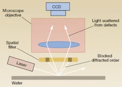
An off-axis laser beam illuminates semiconductor wafer features and defects. Because wafer features form a periodic pattern, they diffract light into orders that can be blocked with a spatial filter. Widely scattered light from the nonperiodic defects passes by the filter and is imaged onto a CCD.
The tester includes a laser, microscope objective, and charge-coupled-device camera (see figure). The wafer to be examined typically contains a regular pattern of features on its surface that acts as a diffraction grating. The laser beam is incident upon the wafer at an angle, unavoidably producing diffracted orders. The key to the NEC device is a spatial filter that blocks the diffracted orders from passing through the microscope, while allowing other scattered light through. Wafers without defects do not produce a signal, but if there is dust or other defects on the wafer surface, the resulting scattered light enters the microscope and produces a signal.
Earlier wafer-testing devices using laser beams have been cumbersome due to the complexity of the optical systems, which contained objective lenses, image-formation lenses, and intermediate lenses. Such wafer testers could not be integrated in a production line and were instead located in separate testing areas.
In the NEC device, the optical detection head has been miniaturized to one-half the weight of a conventional head. The floor area required to install the device is one-fifth that needed for conventional products, allowing it to be placed within the production line. For this reason, test results can be immediately integrated into the production step.
Courtesy O plus E magazine, Tokyo

