Photonic-Crystal Lasers: Photonic crystals promise unprecedented lasers and efficient LEDs
SUSUMU NODA
Photonic crystals, in which the refractive index changes periodically, provide an exciting new tool for the manipulation of photons. Two-dimensional (2-D) photonic crystals are the basis for unprecedented semiconductor lasers with near-perfect single-mode behavior over a large area.1, 2 The lasing principle is based on 2-D coherent optical coupling among the light waves propagating in various directions, which is mediated by the band-edge effect of 2-D photonic crystals.
It can also be shown that spontaneous emission emitted to in-plane 2-D directions is inhibited by the 2-D photonic-bandgap effect. Simultaneously, the stored energy is redistributed to the vertical direction, where this bandgap effect does not exist. As a result, simultaneous inhibition and redistribution of spontaneous emission is achieved within 2-D photonic crystals-a result that is very encouraging for their application to light-emitting diodes with very high extraction efficiency.
Controlling lasing oscillation
It is well recognized in the laser community that when the surface area of a semiconductor laser is increased, a lateral mode becomes multimode, and its operation becomes very unstable. But if a stable single longitudinal- and lateral-mode oscillation can be achieved-even in the case of a large-area semiconductor laser-a completely new laser is realized. Today, 2‑D photonic crystals make it possible to construct such a laser.
In a 2-D photonic-crystal laser, the crystal structure is formed on top of a gain medium or active layer and becomes embedded inside the device as the various layers of the structure are fused together (see Fig. 1). The photonic crystal has a square-lattice structure, and the period of the lattice in one direction is designed to match the light-emitting wavelength of the active layer. In this case, the light wave propagating in that direction is diffracted not only backward (-180°), but also in two orthogonal (±90°) directions, which induces an optical coupling among light waves propagating in four equivalent directions and forms 2-D standing waves (or a 2-D cavity mode). In a band diagram for this laser, the cavity mode is given by the band edges of the four bands, where the group velocity of light becomes zero. From a detailed mathematical analysis, a lasing mode corresponding to one of the band edges has the lowest cavity loss and is likely to oscillate.3, 4 Note that a surface emission occurs in this device because the 2-D photonic crystal also functions as a diffraction grating in the direction normal to the wafer.
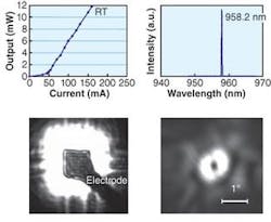
The theoretically calculated band diagram for a fabricated indium gallium arsenide/gallium arsenide (InGaAs/GaAs) photonic-crystal laser with an oscillation wavelength of 900 to 1000 nm agrees well with the measured band diagram. Despite the fact that the area of lasing oscillation is as large as 150 × 150 µm, the power output, lasing spectrum, and near- and far-field patterns show that a stable single-mode oscillation has been successfully achieved (see Fig. 2). The far-field pattern normal to the device displays a unique ring-shaped beam pattern that is based on the electromagnetic field distribution of the lasing mode of the band edge as described previously, and is considered to be important for the development of optical tweezers used to manipulate small, opaque objects. Current research indicates that manipulation of unit-cell structures and/or lattice phases in the crystal can control the shape of the beam pattern.Controlling spontaneous emission
Spontaneous emission is a fundamental factor (or bottleneck) limiting the performance of photonic devices. In light-emitting diodes (LEDs), for example, spontaneous emission that is not extracted from the device contributes to losses. Similarly, in lasers, spontaneous emission that does not couple to the lasing mode results in both losses and noise. Therefore, inhibiting undesirable spontaneous light emission and redistributing the energy into useful forms is very important. At Kyoto University, we have demonstrated that 2-D photonic crystals can inhibit spontaneous emission from a light emitter embedded in the crystal to 2-D in-plane directions; simultaneously, the energy supplied to the light emitter can be redistributed to the vertical direction.5
Spontaneous emission originates from fluctuations in the vacuum field. Under a weak light-matter coupling regime, the rate of spontaneous emission (Rspon) is given by Fermi’s golden rule and is determined by the number of optical modes. The optical modes must somehow be manipulated to control spontaneous light emission.
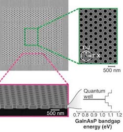
To demonstrate this effect, a triangular-lattice 2-D photonic crystal is formed in a gallium indium arsenic phosphide (GaInAsP) semiconductor slab (see Fig. 3). The structure incorporates a single quantum well (QW) as the light-emitting material, producing light with a transverse-electric (TE) polarization in which the dipole moment is orientated parallel to the slab plane. The optical modes in the thin slab can be categorized into two types: “slab modes” that are confined to the 2-D plane by satisfying the total internal reflection (TIR) condition for the vertical direction, and “vertical modes” that do not satisfy the TIR condition and are emitted outside the slab. Excited carriers that are confined in the QW generate spontaneous emission coupled to both slab and vertical modes, and the spontaneous emission rate can be expressed by Rspon = Rslab + Rvertical. Here, Rslab and Rvertical denote the spontaneous emission rates for slab modes and vertical modes, respectively.For a semiconductor slab with a large refractive index that is surrounded by low-refractive-index air cladding, light is strongly confined within the slab and the condition Rslab >> Rvertical is satisfied, meaning that spontaneous emission from the QW is mostly coupled to the slab modes. However, when a 2-D photonic-crystal structure is incorporated in the slab, Rslab is inhibited, and basically no modification of Rvertical occurs. As a result, a marked reduction in Rspon is expected through the inhibition of Rslab.
The 2-D photonic bandgap is responsible for inhibiting emission into the slab modes so that photons emitted from the QW can couple only into the vertical modes; that is, the quantum efficiency of spontaneous emission in the vertical direction will increase. These simultaneous effects-the reduction of Rspon due to the inhibition of spontaneous emission into 2-D slab modes and the increased emission efficiency of the vertical modes-illustrate how the 2-D photonic crystal effectively redistributes the light energy from the 2‑D plane to the vertical direction.
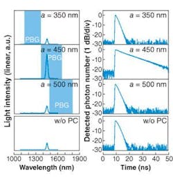
Quantitative experiments to demonstrate this light redistribution to the vertical direction were completed using a series of samples prepared on the same wafer with photonic-crystal lattice periods ranging from 300 to 500 nm in 10-nm intervals. The samples were optically pumped using a titanium aluminum oxide (Ti:Al2O3) laser emitting at 980 nm with a pulse width of 2 ps and a repetition rate of 2 MHz at 4 K. When the emission wavelength is within the photonic-bandgap region, the spontaneous-emission lifetime (which corresponds to 1/Rspon) increases by five times compared with that observed in structures not incorporating photonic crystals (see Fig. 4). In contrast, when the emission wavelength lies outside the photonic bandgap, the spontaneous emission lifetime and the emission efficiency in the normal direction are both comparable to those observed in structures without photonic crystals. These results are qualitatively in good agreement with theoretical analyses, successfully demonstrating the simultaneous inhibition and redistribution of spontaneous emission by 2-D photonic crystals.While this experiment was conducted at low temperature to avoid the nonradiative recombination process, use of a 3-D carrier confinement effect through quantum nanostructures, for example, would allow observation of this effect even at room temperature.
The control of spontaneous emission enabled by 2-D photonic crystals is an important step in the evolution of photonic devices. In particular, it may lead to the drastic increase of the external quantum efficiency of LEDs, which is very important for next-generation all-solid-state illumination systems.
REFERENCES
1. M. Imada et al., Appl. Phys. Lett. 75, 316 (1999).
2. S. Noda et al., Science 293, 1123 (2001).
3. D. Ohnishi et al., Optics Express 12, 1562 (2004).
4. K. Sakai et al., IEEE J. Selected Areas in Communications 23, 1330 (2005).
5. M. Fujita et al., Science 308, 1296 (2005).
Susumu Noda is a professor in the Department of Electronic Science and Engineering at Kyoto University, Kyotodaigaku-Katsura, Nishikyoku, Kyoto 615-8510, Japan; e-mail: [email protected].


