The well-worn term “paradigm shift”—sometimes preceded by the phrase “nothing less than a”—has, for many who have spent time in the corporate world, become not merely empty of meaning, but a symbol of hyperbole. Contrary to what some may think, though, the term was not invented by a motivational consultant. Instead, it was coined by science historian Thomas Kuhn, and popularized in his 1962 book The Structure of Scientific Revolution; the term arose from his views on science and how it progressed—which, he believed, was erratically.
Kuhn maintained that scientists typically (in times of what he called “normal science”) act as puzzle solvers, adding to or tweaking the existing theoretical base, or paradigm. Every once in a while, however, a combination of new data and scientific brilliance can cause a fundamental change in outlook, causing a deep restructuring, or shift, of the paradigm. One example is the change from a Ptolomaic to a Copernican view of the solar system.
While more-mundane acts of restructuring—such as the relocation of an engineering department nearer to the manufacturing area—may be termed paradigm shifts by a company exec, they are most likely not. However, a slight broadening of the term’s original meaning to include radical shifts in thinking relative to technology may not be unwarranted. In the past few years, and especially this past year, the field of optics has been approaching what could be such a shift-that involving the design, development, and possibly the eventual practical use of negative-refractive-index materials in optical systems.
In technology, just as in science, however, fundamental changes in approach mean nothing without the rest of the creative and difficult work needed to make devices suitable for the real world. The vast majority of the advances in photonics and optoelectronics this year have not been paradigm shifts, but are of prime importance nonetheless. So, putting corporate slang aside, perhaps we should simply be grateful for those researchers and engineers who can both work in the trenches and think outside the box.
How strange
To optical engineers, fabricators, and others used to the properties of glass and optical crystals, the idea of a material with a negative refractive index is an alien one. Such materials can be created, however. For example, certain intricate structures with subwavelength features and periods, if constructed from dielectric and metal components, can have negative dielectric permittivity and negative magnetic permeability—and, as a result, negative refractive index. Optical systems containing lenses with unusual properties (for example, focusing done by flat surfaces) could one day be the result; these would give optical designers options never before thought possible. “Superlenses,” which image beyond the diffraction limit by preserving evanescent waves, are another speculative outcome.
Such subwavelength structures, called metamaterials, work best if they have periods on the order of a tenth of a wavelength or less. They can be made relatively easily for use at microwave frequencies, where the structures have periods of a few millimeters or more. But creating metamaterials with features small enough for operation in the visible, or even IR, is a different story. Aided by photolithographic techniques, however, researchers are approaching this goal.
In a technical session at the Optical Society of America’s CLEO/QELS 2005 conference (Baltimore, MD), Stephan Linden, a researcher at the Forschungszentrum Karlsruhe Institut für Nanotechnologie (INT; Karlsruhe, Germany), described the fabrication of arrays of metallic split rings less than 400 nm in width that exhibit magnetic resonance at 3-µm wavelengths (see Fig. 1).1, 2 Developed by a team of researchers from German, American, and Greek universities, the structure allows negative magnetic permeability; the addition of short wires to the structure for negative permittivity could result in a negative refractive index.
Using interferometric lithography at 355 nm, researchers from the University of New Mexico (Albuquerque, NM) and Columbia University (New York, NY) have fabricated a simple metallic/dielectric structure with a 1-cm2 total area that has a refractive index whose real component dips as low as -2 for a narrow range of wavelengths centered on 2 µm (see p. 22).3 A 60-nm layer of aluminum oxide separates two 30-nm layers of gold that are perforated with 360‑nm holes in an 838-nm pitch square array. The structure absorbs light, however-a characteristic of metamaterials in general that may require them to be used in extremely thin layers. But because a hypothetical perfect lens could exist in the form of a flat slab, a thin layer may be adequate.
Negative refractive index can also arise in a photonic crystal, or even in some metals for certain wavelengths. For example, a 50-nm-thick uniform film of silver was used by researchers at the University of Canterbury (Christchurch, New Zealand) as a slab near-field lens to achieve superresolution at 365 nm (see Laser Focus World, June 2005, p. 15). Unlike proximity printing, the highest image resolution occurs a short distance away from the lens, not in contact.
There is even an outside chance that negative-index lenses could be made by mixing two types of dust. Researchers at the University of Edinburgh (Edinburgh, Scotland) and Pennsylvania State University (University Park, PA) have postulated that a homogeneous mixture of two hypothetical isotropic dielectric-magnetic materials, each pulverized to tenth-wavelength-size (or smaller) grains, could form a negative-index metamaterial (see Laser Focus World, November 2005, p. 53). The researchers have no idea yet what these two substances might be, however.
Many research efforts are under way around the world to create metamaterials that operate at shorter wavelengths and show clearer negative-index effects. Improved photolithographic techniques and more-refined nanostructures will eventually lead to a metamaterial that exhibits a negative refractive index in the visible region. In addition, metamaterials showing nonlinear effects (such as frequency doubling) or gain (leading to optics that could not only focus but amplify light) will be developed. Conquering the practical problems of light absorption, difficulty of fabrication, and performance, however, is what will bring metamaterials out from the lab and into your cell-phone camera.
Silicon photonics
Decades of research and development have brought silicon electronic chips from their original single-transistor form all the way to integrated circuits that contain a billion transistors with nanoscale features. Just as important, the associated semiconductor-processing technology has turned silicon into a versatile medium for precision mass-producible devices that include not only electronics, but MEMS (microelectromechanical systems) devices as well.
This year, integrated silicon photonics has moved closer to reality. Silicon’s poor light emission has traditionally frustrated efforts to create integrated optoelectronic circuits based on the material. But in February, researchers at Intel (Santa Clara, CA) revealed the first all-silicon laser on a chip, an S-shaped waveguide Raman laser that, when pumped with pulsed light at 1536‑nm, lased at 1669.5 nm (see Laser Focus World, February 2005, p. 9). The group soon demonstrated a continuous-wave (CW) version, in which a reverse-biased p-i-n diode in the waveguide reduced the optical loss caused by two-photon-absorption-induced free-carrier absorption to the point at which CW operation was achieved. A silicon Raman laser developed by researchers at the University of California at Los Angeles, though optically pumped by pulsed light, can be directly modulated with an electrical signal to a p-n junction diode on the gain chip (see Laser Focus World, April 2005, p. 21).
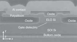
Scientists at Intel have also created a second essential element of a practical silicon photonic circuit (or at least one that would rely on CW lasers): a high-speed silicon optical modulator. Last year, they reached 1-Gbit/s optical modulation for a silicon device in which the refractive index of a silicon waveguide was modulated by a metal-oxide-semiconductor capacitor. The device trounced the previous record by a factor of 50; however, even this is not considered truly high-speed. This year, the researchers revealed a refined version that reaches 10-GHz (see Fig. 2).4 Redesigning the silicon waveguide—for example, changing the top layer from polysilicon to crystalline silicon—and improving other elements such as the driver circuitry allows the device to transmit 10 Gbit/s with a 3.8‑dB extinction ratio and 10 dB of on-chip loss.All these silicon devices operate at or close to a wavelength of 1.5 µm. An alternative approach to silicon photonics, which can operate at shorter wavelengths, is heterogeneous integration. In this case, a light-emitting material other than silicon is layered onto a silicon chip and can potentially be integrated with silica waveguides and ordinary silicon detectors. Andrew Steckl and Jeong Ho Park of the Nanoelectronics Laboratory at the University of Cincinnati (Cincinnati, OH) have fabricated visible lasers on silicon that consist of a 0.5-µm active layer of europium-doped gallium nitride (GaN); when pumped by pulsed 337-nm light, the lasers emit at 620 nm with a threshold of 117 kW/cm2 (see p. 13). Modal gain and loss were 100 and 46 cm-1, respectively. Doping GaN with other rare-earth elements could produce other laser wavelengths in the visible, UV, and IR regions.
High-power light
As the optical output of a solid-state laser is boosted, the standard laser-rod geometry becomes less and less practical-a result of beam nonuniformities and other problems caused by the long thermal path in the rod. To shorten the thermal path, a laser rod can be made either long and thin (a fiber) or short and fat (a disk or slab). Both approaches have their strong points.
In the past couple of years, fiber lasers have undergone an unprecedented growth in power (see Laser Focus World, August 2005, p. 66). The record optical output for a single-fiber laser is currently held by IPG Photonics; in a paper presented at SPIE’s Photonics West 2005 (Jan. 24-27; San Jose, CA), IPG researchers revealed that they had achieved a 1960-W output from a 1075-nm-emitting ytterbium-doped fiber that produced a beam with a quality M2 of 1.2 at an electrical-to-optical (wall-plug) efficiency of greater than 20%. Engineers and researchers from around the world are aiming to push this number higher, though; for example, also at Photonics West 2005, David Payne from the University of Southampton (Southampton, England) discussed techniques for scaling single fibers to 10-kW power levels (see Laser Focus World, April 2005, p. 29).
For multiple-fiber lasers, in which the outputs of many single-fiber lasers are combined in a passive multimode fiber, IPG Photonics again holds the record; in addition to installing a 20-kW fiber laser at the Bundesanstalt für Materialforschung und-prüfung (BAM; Berlin, Germany), the company has also installed a 36-kW laser for an unnamed customer. The laser’s output is delivered by an optical fiber with a diameter of 200 μm, resulting in a beam-parameter product of 11 mm × mrad.
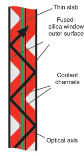
Fiber lasers are limited by the fact that the lasing material must be capable of being drawn into an optical fiber. In contrast, slab and disk lasers can be made from any laser-gain medium that can be ground and polished. For example, ceramic Nd:YAG is three times more fracture-resistant than crystalline Nd:YAG, has a more uniform index of refraction, and can be made into meter-size elements. Researchers at Textron Systems (Wilmington, MA) have built a slab ceramic YAG laser that produces an average power of 5 kW (see Laser Focus World, October 2005, p. 11). A very thin ceramic slab is straddled by two flowing-liquid cells; the beam passes through both cells and slab, resulting in a near-field output with an aspect ratio close to unity (see Fig. 3). The technology is sponsored by the Air Force Research Laboratory (Kirtland AFB, NM) and is intended for weapons-class lasers.But for diode-pumped solid-state weapons-class lasers, especially those that must be compact and lightweight enough to be usable in vehicles, cooling the vast arrays of pump diode lasers can be more difficult than cooling the solid-state gain medium. The pump diodes for a 100‑kW-class laser, for example, can produce two or three times as much heat as the solid-state laser material itself. Lightweight diode-cooling techniques are being developed that can handle these multihundred-kilowatt heat loads.
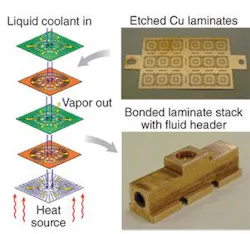
At PennWell’s Military Technologies Conference (March 15-16; Boston, MA), a presentation prepared by Chad Boyack and Kevin Hopkins of Raytheon Missile Systems, and given by Boyack, outlined the latest developments in two-phase cooling, in which a cooling fluid changes to its vapor phase, removing far more heat than a fluid alone could (see Laser Focus World, July 2005, p. 19). The approaches, pursued at Raytheon and elsewhere, include bonded-laminate jet impingement, vapor-injected spray, and slot-jet. For example, bonded-laminate jet impingement techniques being developed at Hamilton Sundstrand (Windsor Locks, CT) for laser-diode cooling are used in the company’s evaporative compact high-intensity cooler (ECHIC), as well as its single-phase version, the CHIC. Stacked and bonded copper foils with complex geometries produce an effective coolant flow (see Fig. 4).
The vision thing
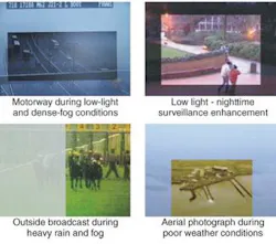
While electronic imaging systems can produce spectacular images for surveillance, machine vision, and other uses, their image-processing and enhancement techniques (and the additional processing that determines what to do with the information) can fall short when judged against the ultrasophisticated performance of the human eye/brain combination. A human can detect and categorize edges and other components of a scene swiftly and naturally, and act on it without much thought-one reason that jet-fighter pilots are not obsolete. Image processing can, however, enhance a scene in ways the human brain can’t.Confronted with a hazy view, for instance, a human mind will try to “reset” the contrast range to make it seem larger than it is (perhaps this occurs successfully as you forget for a moment that you are peering through mist). But the loss in contrast is real nonetheless. A real-time enhancement technology developed at Dmist (Manchester, England)—a spinoff from the School of Electrical and Electronics at the University of Manchester-cuts through haze in a different and more authentic way (see Vision Systems Design, May 2005, p. 18).
Based on known range data, which provides the depth of haze for the algorithm, the Dmist image enhancer separately compensates each red, green, and blue pixel in the color image based on their color. Because scattering can be different for each of the three colors (for example, in bluish smoke or brownish haze), the enhancement produces a higher-quality image than simpler techniques that treat the haze as a monochrome influence (see Fig. 5).Another limitation of the human “hardware” is the fact that the eye has only three types of spectral detectors, centered on red, blue, and green (with overlapping spectral ranges); other perceived colors are the result of the brain’s postprocessing. Thus, while pure yellow light appears yellow to a human, so does a mixture of red and green light. Digital color cameras all follow this principle as well.
For precision spectral analysis, this is an awkward approach, because response and sensitivity vary in a chaotic manner across the visible spectrum. But tunable liquid-crystal filters, with their slowly and smoothly varying response across the spectrum, solve this problem. For example, CRI (Woburn, MA) makes a liquid-crystal filter tunable from 400 to 720 nm (and others with different ranges, all the way out to 1200 to 2450 nm), with apertures up to 35 mm and bandwidth from 0.25 to 20 nm.
This type of filter was used by researchers at the U.S. Department of Agriculture and Michigan State University (both in East Lansing, MI) to nondestructively test fruit texture (see Laser Focus World, April 2005, p. 99). Combined with a monochrome CCD camera and a tungsten-halogen lamp, a liquid-crystal filter with a 650- to 100-nm range enabled measurement of backscattering across the surface of, for example, an apple. Less-firm apples scatter more; the set of four best wavelengths for testing Red Delicious apples is different from the set for Golden Delicious, highlighting the advantage of continuous filter tunability.
While CMOS imagers tend to have more crosstalk than CCD image sensors, scientists at IC Media (Santa Clara, CA) have determined that, in some cases, crosstalk in CMOS devices may not be as much of a problem as previously thought (see Laser Focus World, January 2005, p. 119). Color-reproduction quality, which normally suffers when crosstalk is present, can be compensated by adjusting the spectral transmission curves of the CMOS device’s color filters. The design of the filters arises from complex calculations that take into account the CMOS quantum efficiencies, microlenses, and spectral-response shifts resulting from crosstalk, which are modeled on silicon parameters. The optimized filters provide better overall color reproduction than can be achieved with standard filters.
Ultrafast gets a prize
Attosescond pulses, which can only be produced from light that spans a huge spectral range extending into the vacuum UV, are short enough to enable scientific exploration of the atom’s inner workings, including its electronic transitions (see Laser Focus World, October 2005, p. 103). This large spectrum is produced by the interaction of a few-femtoseconds-long laser pulse with a gas. Single reproducible attosecond pulses can be created by aligning the electric-field phase of the generating pulse with the peak of the amplitude envelope (see Laser Focus World, July 2005, p. 75). Such achievements jointly earned scientists John Hall of JILA (Boulder, CO) and Theodor Hänsch of the Max Planck Institute for Quantum Optics (Garching, Germany) half of this year’s Nobel Prize in physics (see Laser Focus World, November, 2005 p. 11). (The other half was awarded to Roy Glauber of Harvard University [Cambridge, MA] for his quantum-mechanical theory of optical coherence.)
Apart from creating such exotic spectra, other approaches exist for shortening ultrafast pulse lengths that are extensions of current femtosecond technology. At the 2005 annual meeting of the Massachusetts Institute of Technology’s Center for Integrated Photonic Systems (MIT CIPS; Cambridge, MA), Franz Kärtner of MIT described experiments aimed at the coherent superposition of two separate modelocked lasers-one Ti:sapphire and the other Cr:forsterite-to create a spectrum spanning 650 to 1450 nm (see Laser Focus World, August 2005, p. 21). Being much broader than what either laser can produce alone, this spectrum will enable proportionally shorter pulses.
Researchers at the National Institute of Technology and Standards and the University of Colorado (Boulder, CO) have used femtosecond laser pulses to observe the details of half-picosecond-long atomic collisions in dense potassium vapor, confirming theories about how the atoms collide.5 In transient-four-wave-mixing (TWFM) experiments, effects of a 70-fs pulse from a Ti:sapphire laser on the vapor (actually two pulses-an excitation pulse and a probe pulse) show alterations, or “dephasing,” in the initial 500 fs of the TWFM signal, pointing to the atoms losing their form when they hit each other (see Fig. 6).Other exciting areas of photonics and optics research this year include nanophotonics (see, for example, the special report in Laser Focus World, August 2005, p. 73); slow light (Laser Focus World, June 2005, p. 42; August 2005, p. 73; and November 2005, p. 18), and surface-plasmon devices, which in addition to their many uses in biosensing (currently their most well-developed area of application) are enabling, for example, more-efficient LEDs and OLEDs (Laser Focus World, September 2005, pp. 17 and 36).
Selections from the marketplace
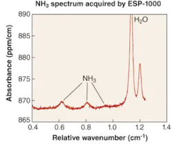
Innovative commercial products abound this year. For example, Picarro (Sunnyvale, CA) introduced a trace-gas-measurement instrument that it claims is the first commercial device that fully exploits cavity-ring-down spectroscopy (CRDS). In CRDS, an optical cavity with very high-reflectance mirrors is filled with the substance under test (typically a gas); a tunable laser pulse enters the cavity and its time-based decay is monitored, providing a sensitive measure of absorption by trace substances (see Laser Focus World, January 2005, p. 35, and March 2005, p. S7). The technique is immune to laser intensity fluctuations.
Picarro’s instrument measures the concentration of ammonia, hydrogen sulfide, acetylene, carbon dioxide, and other gases at parts-per-billion levels (see Fig. 7). Light from a distributed-feedback (DFB) laser enters the cavity, which is adjusted in length to bring the laser and cavity into resonance (the cavity increases the path length by a factor of more than 20,000). When the intensity in the cavity builds up to a high-enough level, the laser is turned off and the ring-down time monitored. Software calculates the absorbance of the gas at that wavelength; the DFB laser is then swept through other wavelengths and the process repeated.TeraView (Cambridge, England), the company that launched the first commercial terahertz spectrometer, has expanded the capabilities of its instrument to include reflective as well as transmissive sampling geometries. The instrument can operate in attenuated total reflection (ATR, in which an evanescent wave arising from total internal reflection probes the sample), specular reflection, and transmission. In the ATR mode, the optical material within which total internal reflection occurs can be switched from germanium to silicon, changing the depth of the evanescent field and thus the probe depth. The tool is useful in the research and development of drugs.
Cobolt (Stockholm, Sweden) introduced a dual-line compact diode-pumped solid-state laser that emits 491- and 532‑nm wavelengths simultaneously, with 20 mW in each color; two media in the same laser resonator result in intracavity frequency mixing in a periodically poled crystal of potassium titanyl phosphate (see Laser Focus World, April 2005, p. 11). The company is working on triple-wavelength versions.
At Photonics West 2005, Newport (Irvine, CA) introduced a series of isolation optical tables with active vibration control; the tables contain vibration sensors and electromechanical vibration dampers that introduce damping into vibration modes without creating low-frequency resonance (unlike ordinary optical tables, which move around quite a bit in the hertz range). The tables can be quickly retuned for optimal damping under changed conditions. The isolation systems’ analog controller and vibration-sensor outputs can be monitored by the user (or, more likely, the user’s computer) for starting or stopping sensitive processes in, for example, optics manufacturing or laser micromachining.
Also at Photonics West 2005, Sydor Instruments (Henrietta, NY) introduced the ROSS streak camera, an instrument initially developed at the University of Rochester’s Laboratory for Laser Energetics (LLE; Rochester, NY). Not only does the stand-alone streak camera have comprehensive autofocus and self-calibration capabilities, but it also has temporal resolution of 12 ps, a dynamic range of 500 for a 2-ns window, a 40-µm (full width at half maximum) line-spread function, and greater than 20-lp/mm contrast transfer function-twice that of existing streak cameras.
At Laser Munich 2005 (June 13-16; Munich, Germany), Fianium (Southampton, England) introduced a supercontinuum source based on the use of high-nonlinearity photonic-crystal fiber and pumped by the company’s high-power ultrafast fiber lasers (see Fig. 8). The source delivers an average power of up to 5 W and spectral power density approaching 5 mW/nm spanning a spectrum from below 430 to greater than 1800 nm with diffraction-limited beam quality over the entire spectrum. The compact fiber pump laser results in a small package size of 250 × 220 × 80 nm.Uses include optical-component characterization, optical-coherence tomography, confocal microscopy, time-resolved fluorescence spectroscopy, and high-definition visual displays.Eastman Kodak (Rochester, NY) has introduced image sensors for professional photography that up the ante in the megapixel race. The company introduced two CCD image sensors for medium-format professional photography with 39 and 31.6 megapixels; their imaging areas are 36 × 48 mm and 33 × 44 mm, respectively, both with 6.8-µm pixel sizes. The sensors have been selected by camera maker Phase One (Copenhagen, Denmark) for use in its upcoming digital-camera backs.
A niggling but longstanding problem in optics fabrication has been remedied by Tekna-Seal (Minneapolis, MN), which has developed a nonoxide hermetic-sealing process that, when used with metal-injection-molded components from FloMet (DeLand, FL), allows hermetic sealing of high-quality optical glass to metal frames (see Laser Focus World, April 2005, p. 9). The traditional glass for this purpose, Corning 7056, seals well but has an uneven transmission spectrum and can contain bubbles; the new process allows uniform glasses such as Ohara S-BAL to be used for optical experiments that require light beams to be coupled into and out of vacuum-tight chambers.
REFERENCES
1. S. Linden et al., CLEO/QELS 2005 technical session JThC1.
2. S. Linden et al., Science 306, 1351 (Nov. 19, 2004).
3. S. Zhang et al., Phys. Rev. Lett. 95, 137404 (Sept. 23, 2005).
4. L. Liao et al., Optics Express 13 (8) (April 18, 2005).
5. V.O. Lorenz and S.T. Cundiff, Phys. Rev. Lett. 95 (16) (Oct. 14, 2005).
About the Author
John Wallace
Senior Technical Editor (1998-2022)
John Wallace was with Laser Focus World for nearly 25 years, retiring in late June 2022. He obtained a bachelor's degree in mechanical engineering and physics at Rutgers University and a master's in optical engineering at the University of Rochester. Before becoming an editor, John worked as an engineer at RCA, Exxon, Eastman Kodak, and GCA Corporation.
