MICRO-OPTICS: Micro Optics technology fulfills its promise
JYRKI SAARINEN, MARKUS ROSSI, AND MICHAEL T. GALE
Major design advances and manufacturing technology improvements for micro-optic components and systems have facilitated the trend toward miniaturization in optics. Up to the mid-1990s, micro-optics development was primarily for military and defense applications requiring components with small size and low weight. With the introduction of high-quality micro-optic components produced by UV embossing and microinjection molding technologies, as well as dramatic developments in materials, these replicated components can now comfortably withstand the harsh environmental requirements of the consumer electronics industry, including IR reflow and thermal shock.
By their very nature, micro-optic components have a typical footprint of only a few square millimeters and are usually less than 1 mm thick, making them ideal for applications in which space is at a premium. In addition, millions of components per month can be manufactured with high reliability and precision. So, it is easy to see why cost-effective micro-optic components are now fulfilling their promise by replacing conventional optics in common products like mobile phones, light-emitting-diode (LED) lighting, and flat-panel displays.
Micro-optics span the entire gamut from diffractive to refractive behavior. At one end lies the refractive microlens with weak wavelength dependence and optical performance determined primarily by the feature profile and depth. At the other end lies the diffraction grating or hologram with highly wavelength-dependent properties and optical performance determined strongly by the lateral feature dimensions and less by the feature depth. In between is a continuous transition from diffractive to refractive behavior, allowing the designer a high degree of freedom to optimize a component for a given application.
Refractive microlens arrays are well suited for broadband illumination and achieve very high efficiency with virtually no stray light. Diffractive lenslet arrays can offer highly accurate and uniform focal-length distribution. Most diffractive optical elements (DOEs) have no equivalent in classical optics. They offer new functionality and have generated a host of new application areas such as pattern generation and complex beam shaping. One example is the generation of the complex pattern of a virtual laser keyboard for use with personal data assistants (PDAs) and mobile phones (see Fig. 1). The DOE used in this example has feature sizes down to 400 nm and achieves an opening angle of over 75° with high efficiency.
Unique to micro-optics
An important and distinguishing feature of micro-optic components is their small size coupled with flatness. The surface-relief feature depth of DOEs is typically in the range of a few hundred nanometers to a few micrometers. Even refractive microlens arrays typically have relief depths of less than 100 µm. This enables production technology not possible for conventional optics, such as wafer-scale ultraviolet (UV) embossing.1 In general, the use of replication technology such as UV embossing, injection molding, and hot embossing for mass production of surface-relief DOEs leads to major cost advantages as the component volume increases. The attraction of a DOE for an optical system, particularly for consumer products, depends upon a successful optimization of the design, mastering, tooling, and production steps; this typically requires a close interaction between the DOE producer and the product developer.
Consumer products, which can be broadly characterized as products produced in large quantities for nontechnical users, represent an ideal industrial segment for micro-optic components and systems. The rapid growth in the use of LED and laser-diode sources as well as CCD and CMOS sensors in consumer products strongly favors micro-optics, whose small size and flexible beam-shaping properties make them ideal partners for these miniature, modern light sources and sensors.2
Designing for production
Today’s designer of micro-optic components and systems will use a combination of commercial and proprietary design and modeling programs, depending upon the detail and feature size of the component. Ray-tracing programs are suitable for purely refractive structures, but diffractive structures require analysis using scalar diffraction theory for coarse features or rigorous diffraction theory for features with dimensions approaching the wavelength of the illumination.
Examples of the major progress achieved in recent years can be found in the design of beam-shaping micro-optics for LEDs. Although typical LEDs are incoherent, spatially extended, and spectrally broadband sources, sophisticated micro-optic designs with a wide variety of optical functions can spectrally and spatially improve the LED output leading to more-compact LED modules.3
In many cases the production technology dictates the achievable precision and limitations, and major progress in recent years means that design approaches automatically take into account the fabrication tolerances and manufacturing constraints. Unlike conventional optics, the design and fabrication phase cannot be separated for micro-optics. An optimal design represents not only an in-depth understanding of micro-optics theory, but also a detailed knowledge of the whole production chain. For replicated micro-optics, rapid prototyping often can be realized by direct laser-beam writing in resist, fabrication of a mold, and replication into UV-curable epoxy with a lead time of only days. This design-for-manufacturing capability supports the drive for fast time-to-market in consumer electronics. Designs can be turned into manufacturable prototypes in a few weeks and a weeks later high-volume production can be achieved.
Wafer-scale replication matures
Replication technology is ideal for the high-volume production of most micro-optic components. The traditional fabrication by etching fused silica is relatively expensive and only suitable for applications with severe environmental or stability requirements, although it is still invaluable for producing the master structure from which a replication mold is fabricated. Master microrelief structures can also be fabricated by direct-writing technologies. Laser-beam writing in photoresist is a rapid, cost-effective technology for continuous and binary relief structures with feature dimensions down to about 1 µm and profile depths in excess of 40 µm. E-beam lithography is especially suitable for binary structures with feature dimensions down to less than 400 nm. So-called recombination technologies, such as step-and-repeat UV embossing, can also be used to build wafer-scale tools from single components.
The main replication technologies for micro-optics can be grouped into three categories: UV embossing, microinjection molding, and hot embossing.
UV embossing involves replicating from a mold into UV-curable epoxy on a glass or other substrate. A major advantage of using epoxy is in the robust nature of the material-certain epoxies have excellent thermomechanical stability and withstand IR reflow (even lead-free processing up to 280°C). High-quality components can be fabricated very economically, in particular at medium to high volumes (thousands to millions of components per month). The thin epoxy layer (minimum of 10-µm thickness) on a substrate such as a glass wafer, silicon (for detectors), or gallium arsenide (GaAs; for emitters) results in a high-quality, stable replica with excellent replication of feature sizes down to hundreds of nanometers. Recent developments include double-sided wafer-scale replication and overmolding.
Microinjection molding is production by injection molding in thermoplastic polymer. Particularly suitable for individual components complete with mounting and packaging features, this technology has relatively high tooling costs and is best for medium-volume series production. There are also materials limitations for subsequent processing and usage at high temperatures and harsh conditions.
Hot embossing in metallized polymer foil is used for diffractive foil and security holograms. This technology is suitable for foil and label applications, but not for high-performance DOE or lenslet array production with tight flatness and microstructure fidelity requirements.
Advantages of UV embossing
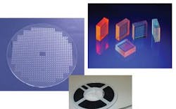
Double-sided and aligned wafer-scale UV embossing has been developed at Heptagon’s production facility near Zurich, Switzerland. This process, referred to as REEMO, is an extension of the standard UV-replication process to large-area glass or optoelectronic wafers. Micro-optic elements are replicated in custom UV-curable epoxy with a layer thickness below 20 µm and a surface planarity better than 1 to 2 µm (see Fig. 2). Thicker layers (up to 200 µm) are also possible for refractive microstructures. The current 6-in. wafer size will soon be extended to 8-in. The wafer can be further processed with thin-film optical coatings, and then diced into individual micro-optic components. This production line has been optimized and automated. With a capacity of several million components per month, it now yields high-quality and low-cost micro-optic elements.
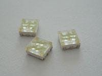
Ultraviolet replication can also be performed directly onto processed dies, for example, in fabricating a micro-optic component on a CMOS or CCD sensor, an LED chip, or other optoelectronic component. Known as overmolding, this technique is very attractive for the production of optoelectronic modules on the wafer level since no additional optics assembly or alignment is required. The UV-curable replication material is dispensed, embossed, and cured directly on the substrate containing optoelectronic components. Unlike most products replicated on glass wafers, accurate control of layer thickness is crucial for these applications. Because the REEMO replication process does not require additional heat or pressure, the optoelectronic chip is not damaged. The approach works equally well for single-die and multi-die solutions. Even when using discrete micro-optic components on a glass substrate, very compact LED illumination modules can be fabricated (see Fig. 3).❑
REFERENCES
1. H. Rudmann and M. Rossi, Optical Engineering 43, 2575 (2004).
2. M. T. Gale, Proc. SPIE 5177, 1 (2003).
3. M. Rossi and M. T. Gale, LEDs Magazine (July 2005).


