Designing an imaging apparatus for the ultraviolet is essentially an exercise in avoiding sharp transitions in material behavior.
Imaging in the ultraviolet presents numerous complications because many optical materials stop transmitting as the wavelength gets shorter until, finally, only reflectance works. But, because an increasing number of image sensors are capable of UV imaging, and because UV imaging reveals many interesting industrial, medical, and scientific phenomena, the need for high-performance, cost-effective UV-camera designs continues to increase. Successful execution of UV-imager design requires careful consideration of the characteristics of optics, sensors, and the radiation.
The ultraviolet spectrum
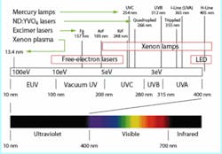
Ultraviolet refers to electromagnetic radiation occupying the wavelength range from just shorter than the visible (about 400 nm) to about 10 nm, where the photons begin to penetrate materials enough to be called soft x-rays. Certain practical effects subdivide the UV spectrum into five bands (see Fig. 1).
Ultraviolet A (UVA) is the tanning and black-light UV band. It passes through most optical materials, as do visible wavelengths, and can generally be detected by visible-light detectors. Although it is invisible to humans, many insects use UVA images to identify certain plant materials, which are highly reflective in this band. Above 340 nm, UVA is commonly used to stimulate visible fluorescence.
Ultraviolet B (UVB) is the sunburn and “solar blind” ultraviolet band. Most UVB is blocked by ozone in the Earth’s atmosphere. In small doses, it produces vitamin D but more exposure causes sunburn and other skin damage. Any intense UVB must come from local sources. Solar-blind imagers, which respond only to the UVB band, permit monitoring of local sources like hydrogen flames and electrical corona in daylight. Some local sources, such as quartz halogen bulbs, can emit enough UVB to pose significant skin hazards.
Ultraviolet C (UVC) is the industrial and germicidal UV band. Solar UVC is almost entirely blocked by ozone, but large amounts of UVC are produced artificially-primarily by mercury lamps emitting at 253.7 nm. This UV band is used extensively for curing, sterilization, and erasing erasable-programmable read-only memories (EPROMs). Glasses largely block UVC so quartz or other materials are needed for optics in this band.
The wavelength boundaries between these three bands are based on photobiological activity and may vary in different references.
Below 200 nm, water vapor and oxygen begin to absorb UV strongly, relegating use of such wavelengths to evacuated systems. Absorption of similar magnitude by one or more atmospheric gases continues down to about 10 nm, so this entire band is called vacuum-UV (VUV). A further designation of the below-100-nm band as extreme-UV (EUV) has been made to indicate that there are no transmissive optical materials useful below 100 nm.
The lower end of the EUV band is being developed for use in semiconductor photolithography. Entire conferences are now dedicated to this topic and its Byzantine complexities. We will say no more here about imaging below 100 nm except to note that reflective optics are required for all operations.
Sensing UV images
Fortunately, silicon can be made to work well as a UV detector across all of the UV bands. When photons enter silicon, they generate hole-electron pairs with nearly 100% efficiency. To generate a signal, one of these carriers must be conveyed to a location where it can be collected for readout. Unfortunately, as the wavelength drops, so does the characteristic radiation penetration distance into the silicon material before absorption occurs. Eventually, the distance gets so short that surface effects on the silicon can draw a substantial proportion of the charge towards the surface instead of allowing it to travel inward to the collection point. The minimum distance, about 25 nm, occurs around 254 nm in wavelength.
Treatments have been developed to provide an electric field in a favorable direction at the surface of the silicon. These can use very thin silver layers or chemisorption techniques, but only work where the unoxidized surface of the silicon can be presented for treatment. As a result, they are generally only applied to backside-thinned scientific imagers.
Careful design of photodiodes can extend useful response below 200 nm for applications in spectroscopy but these are used primarily in line-scan -devices. Frontside area imagers with useful native-UV response below 300 nm are rare. In typical CCD imagers, the photosites are covered with polysilicon electrodes needed to move the charge. The polysilicon is thick enough to absorb essentially all radiation below 400 nm before it reaches the photodiode. Techniques have been devised to provide electrodes without covering the entire photosite or to replace polysilicon with less UV-absorptive materials to improve UV response. With these, the response has been pushed below 350 nm.
One time-tested technique has been to coat the sensor with a transparent phosphor film that converts incoming UV into visible radiation that the sensor can readily detect. This technique is applicable to any sensor. These coatings have been demonstrated to extend response to below 100 nm. They can have negative impacts on overall quantum efficiency (QE) and uniformity.
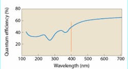
Because the reflectance of uncoated silicon can rise to more than 60% in the 200- to 300-nm range, the maximum possible external QE can be quite low (see Fig. 2). Generally, the surface of the silicon is covered by silicon dioxide, but that offers little help because its index of refraction is too low to form a matching layer. Hafnium oxide (HfO2) is a higher-index material that works well but is practical only in large-area applications with backside-thinned sensors. With field generation and antireflection applied, sensors with external QE in excess of 50% at 300 nm can be routinely made.
Around 340 nm, the photon energy equals the pair-creation energy in silicon, so that at shorter wavelengths two electron-hole pairs are generated and the internal QE exceeds 1. A second extra carrier pair is generated at 170 nm and an additional pair for each incremental 3.7 eV of photon energy. Because this extra charge does not improve the shot noise statistics, it can use up storage capacity in sensors without delivering the signal-to-noise ratio (S/N) expected of strong signals. As a result, storage capacity must be carefully considered for imaging in the VUV.
UV optical materials
Many transmissive materials used in visible optics will also transmit in the UVA band but exhibit a higher index of refraction. This displaces the focal plane forward in most commercial lenses, perhaps a tolerable accommodation. However, most currently manufactured commercial lenses do not transmit well in the UVA band because their antireflection coatings reject wavelengths below 400 nm quite strongly. This is intentional, to avoid fogging of film or bleaching of color-separation filters in still and video cameras. For best performance in the UV, optics must be carefully selected or specially built.
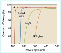
Lenses of many standard glasses can be used down to 300 nm if the AR coatings are designed for UV transmission. Below 300 nm, the choices become much more limited. The primary material used below 300 nm is fused silica, which has useful transmission to below 190 nm, thereby including the ArF laser emission at 193 nm used extensively in semiconductor photolithography. Fluoride doping of fused silica can extend its lower end to nearly 150 nm. All of the other useful materials are crystalline and birefringent to varying degrees. Several common materials can be used below 200 nm (see Fig. 3). Other fluorides, chlorides, and bromides are also useful. Because most of these are soft and hygroscopic, they must be handled very carefully and shaped using special techniques. Optical designs using these materials must include compensation for birefringence.
Multispectral imaging strains lens design capabilities. With silicon imagers and fused--silica optics, the entire band of 200 to 1100 nm could be imaged in air; however, providing adequate correction for optics over this 5.5:1 wavelength range is not feasible. Instead, multiple detectors on a splitting prism are more practical. Up to five channels can be supplied in this way, allowing such combinations as UV, RGB color, and near-IR. The imaging lens would be designed with UVC transmissive materials to provide apochromatic focusing for the RGB section while the focal planes for the UV and IR sections would be slightly offset. Trim filters on those two ports could restrict the outputs to a narrower band of interest.
Reflective optics are also useful in the UV. Below 100 nm they are mandatory, but even at longer wavelengths they have a place. Gold and silver, common reflecting materials used in the visible and IR, perform poorly in the UV-aluminum is the material of choice. Typical aluminized mirrors used for astronomy will reflect about 85% of UV light as long as they have not been coated with protective layers that absorb UV. Objectives for UV microscopy that incorporate two aluminized surfaces have long been available. ❏
DAVID GILBLOM is president of Alternative Vision Corporation, PMB 263, Suite 121, 5575 E. River Road, Tucson, AZ 85750; e-mail: [email protected].


