Photonic crystals offer a host of possibilities
The concept of the photonic crystal offers tremendous promise-the challenge is to realize that promise in practical devices.
The fertile concept of the photonic crystal is spawning a new generation of optical devices that confine light using internal microstructures. The best-known class of devices is fundamentally among the simplest-holey fibers-which are waveguides that confine light inside the fiber so it propagates in a single direction. Yet the most exciting possibilities lie in more-complex devices such as splitters, junctions, and optical microcavities that can be the building blocks of micro-optical circuits. Development is still in the early stages, but the results look encouraging.
The photonic-crystal concept
Photonic crystals are materials in which internal microstructures create period variations in the dielectric constant on the scale of a wavelength of light. Holey fibers, for example, are made by fusing together a bundle of glass tubes and drawing the heated bundle to produce a thin fiber with fine holes running along its length. A two-dimensional (2-D) example is an array of regularly spaced vertical rods standing in air or-equivalently-regularly spaced holes in a solid. In each case, the difference in dielectric constant is between air and the transparent solid, but it is also possible to fill the holes with fluid to alter the dielectric constant and properties of the photonic crystal.
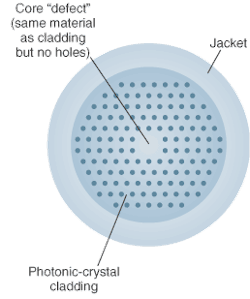
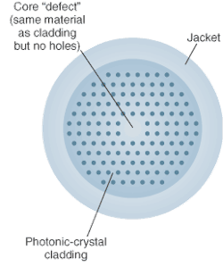
Bragg scattering from the dielectric interfaces blocks some wavelengths from propagating in the microstructure, creating a photonic bandgap that’s an optical analog of the gap between the valence and conduction bands in semiconductors. The microstructure is then totally reflective at these wavelengths, although the two materials that combine to form the structure are transparent. This makes it possible to confine light in a “flaw” in the microstructure, such as a zone of solid glass or empty space (see Fig. 1).
The structures must be smaller than the wavelength, so the concept initially was demonstrated with microwaves and structures scaled to their wavelength. Reducing the dimensions to optical wavelengths followed, although it posed a challenge for some structures. Microstructured fibers were relatively easy to produce by stacking together rods and tubes and drawing them to finer diameters using well-established bundle-fabrication technology.
Photonic crystals allow things that are impossible with conventional solid fibers, such as confining light in the hollow core of a “photonic-bandgap” fiber. In this case, the core is an air hole surrounded by a layer of photonic crystal material with holes running along the length of the fiber. Light at certain wavelengths cannot enter the photonic crystal, so it is guided through the hollow core, but wavelengths outside the photonic bandgap can leak out. This effect can’t be explained by classic optics because the refractive index of the photonic-crystal material is higher than that of the air core. Solid-core “photonic-crystal fibers” are different, because the holes in the photonic crystal surrounding the solid core reduce its refractive index below that of the solid, so their light guiding can be explained by total internal reflection.
Passive planar devices
The same principles can be used to make planar waveguides, but the real payoff is in fabricating more-complex devices in planar waveguides, including splitters, couplers, and filters. The fundamental problem is to fabricate practical microstructures.
The first demonstration was with a 2-D array of regularly spaced vertical rods designed to reflect millimeter waves. Experiments confirmed theoretical predictions that the millimeter waves would be trapped in a slot where the rods had been removed. If rods were removed to create a waveguide that bent 90°, the waves would turn the right angle with very little loss-something that’s impossible with ordinary optics. Since then the same effects have been demonstrated at optical wavelengths and new devices have been developed.
Low-loss splitters have been difficult to make because the waveguide discontinuities needed to divide the light can excite higher-order modes and introduce reflections. In July, a team at the Technical University of Denmark in Lyngby reported a low-loss version by forming a Y junction with 60° bends in the single-mode waveguide.1 The photonic crystal is a 220-nm silicon layer, deposited on silica, with an array of holes spaced on a 435-nm grid. The team fabricated the waveguide stripes by omitting the holes, and added larger holes and rearranged smaller ones to guide the light around the bends in the 15 × 20-µm device. The researchers report no extra loss-compared to a straight section of waveguide-for a 3-dB splitter operated at 1560 to 1585 nm.
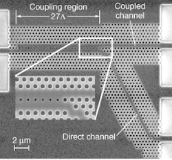
Earlier, the Lyngby group reported making a directional coupler using a similar array of holes in silicon on silica. In this case, they transferred light from a through waveguide to a coupled channel; both formed by removing a row of holes (see Fig. 2). A single line of 27 smaller holes on the same spacing separated the two channels in the coupling region, then the coupled channel branched off at an angle. They report that coupling was both efficient and uniform over a range of wavelengths, with output of the coupled channel -1.3 dB ±0.3 dB down from the input between 1450 and 1490 nm.2
Dispersion effects
Another unusual property of planar photonic crystals is called the “superprism effect,” a very high angular dispersion of wavelengths. Early work showed that the angular spreading, which depended on group velocity, could spread light differing by only about 1% in wavelength over a 50° range of angles.3
This effect is being investigated for applications in light-deflection devices based on changing the wavelength or angle of incidence. Dispersion in photonic crystals also could be used for various types of beam splitting. One proposal envisions fabricating a beam-splitting photonic-crystal region at a 45° angle to the input light; the design of the splitting region determines how much light emerges from two ports.4
The dispersion properties of photonic crystals also can create a waveguide effect that does not require forming a waveguide structure.5 In this case the structure’s dispersion properties are engineered so light can propagate only in certain directions through the structure. Potential applications include routing signals so they cross each other without inducing crosstalk.
Photonic crystals also display polarization dispersion, which has been used to separate vertical and horizontal polarizations by 10° when they passed through a 20-µm length of photonic crystal.6
Laser cavities
The ability of photonic crystals to trap light in a defect zone also can be used to create resonant cavities for storing light and for laser oscillators. Potential applications include studies of cavity quantum electrodynamics and development of quantum optical devices with capabilities including emitting a single photon on demand. The best results so far have come from planar photonic crystals, but progress has also been reported on 3-D structures.
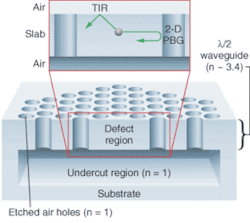
A planar photonic crystal could be an array of holes fabricated in a diode-laser material such as indium gallium arsenide phosphide (InGaAsP; see Fig. 3). The laser zone is a defect in the center of the photonic crystal where the hole is missing or different from the surrounding material. Typically, optical pumping produces emission in the laser defect at a wavelength in the photonic bandgap. The photonic crystal confines light horizontally, while conventional wave-guiding confines light vertically. The emitted light escapes through the waveguide surface or by tunneling through the photonic crystal.
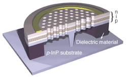
The first planar photonic crystals in 1999 were pulsed devices that operated at 143 K, with a cavity Q factor estimated at 250.7 Great strides have been made since then, including room-temperature operation and Q factors above 10,000.8 In September last year, the first electrically driven planar photonic-crystal laser was reported by a team at the Korea Advanced Institute of Science and Technology in Daejeon.9 The current passed through a semiconductor post that contacted the defect on the bottom, and a ring electrode on top (see Fig. 4). That design has relatively high resistance because the base contact is thin and the ring is far from the laser defect, but the researchers report a threshold current of 260 µA. That’s a significant step toward ideal goals such as a zero-threshold laser or a single-photon source, although many challenges remain, including developing ways to inject single electron-hole pairs into the cavity and to couple coupling light more efficiently out of it.
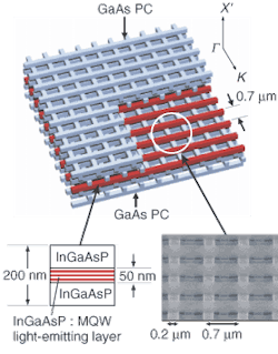
Three-dimensional photonic crystals could be more attractive in the long term because they promise better confinement and more complete blocking of emission in the bandgap. However, it’s been hard to make them with the point defects needed for microcavities or lasers. Last year, a team at Kyoto University succeeded using a “woodpile” structure made by arranging thin sticks of gallium arsenide to make a multilayered lattice (see Fig. 5).10 The sticks, 0.2 µm wide and set on a 0.7-µm grid, formed a photonic crystal. Multiple-quantum-well structures of InGaAsP served as the defects in the stacked lattice. The Kyoto group confirmed the presence of defects, and optical pumping produced 1.55-µm emission concentrated at the defects, while the photonic crystal remained dark at that wavelength.
Outlook
Developers have much work left to implement the host of ideas already proposed by theorists. It can be tough to fabricate devices that reproduce the behavior of electromagnetic fields simulated by sophisticated computer models of photonic crystals. Fibers and planar photonic crystals are relatively easy because their fabrication can draw on years of experience in fiber drawing and semiconductor processing. Three-dimensional structures are more difficult.
Yet 3-D structures also promise entirely new capabilities. Theorists predict that 3-D photonic crystals could be made with negative refraction, offering potentially revolutionary optical properties. The tiny scales required at optical wavelengths pose a major fabrication challenge, and no one knows how to make most of the proposed structures. However, one structure proposed in November is designed to be compatible with interference lithography, although it has not yet been fabricated.11
The challenges that remain are to make the transition from a hot research field to a practical technology and to match the capabilities of photonic-crystal devices to application requirements. Can actual devices live up to the promise of theoretical models? What problems can photonic crystals solve? There’s plenty to look forward to. ❏
REFERENCES
1. L. H. Frandsen et al, Optics Lett. 29, 1623 (July 15, 2004).
2. M. Thorhauge, L. H. Frandsen, and P. I. Borel, Optics Lett.28, 1525 (Sept. 1, 2003).
3. Hideo Kosaka et al, J. Lightwave Tech. 17, 2032 (November 1999).
4. S. Shi et al, Optics Lett. 29, 617 (March 15, 2004).
5. D. W. Prather et al, Optics Lett. 29, 50 (Jan. 1, 2004).
6. L. Wu et al, Optics Lett. 29, 1620 (July 15, 2004).
7. O. Painter et al, Science 284, 1819 (June 11, 1999).
8. M. Loncar et al, Optics Lett. 29, 721 (April 1, 2004).
9. H-G Park et al, Science 305, 1444 (Sept 3, 2004).
10. S. Ogawa et al, Science 305, 227 (July 9, 2004).
11. X. Ao and S. He, Optics Lett. 29, 2542 (Nov 1, 2004).
