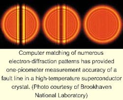
Coherent electron diffraction may eventually become a standard design and quality-assurance tool for perfecting material defects during the manufacture of semiconductor integrated circuits and high-temperature superconductors. Researchers at Brookhaven National Laboratory (BNL; Upton, NY) have used a custom-designed transmission electron microscope to generate holographic shadow images of a stacking fault within a thin crystal of a high-temperature superconductor, which enabled them to measure the defects with an accuracy of one picometer.1
Since structural irregularities are actually what make semiconductors and high-temperature superconductors functional, the ability to measure these defects precisely is expected to impact the understanding of these materials as well as capabilities for design and manufacturing, according to Yimei Zhu, a member of the BNL research team.
"In structural materials that might be used for building bridges, defects actually weaken the material," he said. "But for functional materials defects are a different issue."
The types of defects that Zhu studies include the irregularities in high-temperature superconductors that "pin" flux lines in place and help the materials carry high currents, and the dopants in semiconductors that affect the interaction between charges and holes, as well as the functioning of quantum wells and quantum dots.
"Usually we don't understand defects that well because they're very small and difficult to detect," Zhu said. "So we just put materials together and are pleased when they work. But if we can understand defects with very high resolution then we will be better able to design materials or devices."
The precise measurement method is based on the use of a coherent electron beam generated by the field emission gun on a 300-kV transmission electron microscope, as opposed to the conventional method of heating a filament to produce an incoherent electron beam. Zhu's team then used the prespecimen lenses of the microscope to position the source and generate interference patterns.
"Usually if you use a convergent beam you basically focus the beam on the sample," he said. "But we did not focus the beam on the object: we focused the beam above the object and we obtained shadow images in which we saw the illuminated areas as well as diffraction."
The coherent electron beam allowed the researchers to extend their observations out to 31st order reflections, which were then analyzed using computer simulations. A measurement accuracy was obtained on the order of 0.001 nm, equivalent to a magnification factor of about 50 million.
"If we magnify an atom at one-angstrom resolution, then the atom will be a ping-pong ball on the screen," he said. "And if we magnify the ping-pong ball 50 million times it would be like the size of the earth. And actually, we're talking about a hundredth of an angstrom, so it's even smaller."
The next step for the BNL team will be to look for additional applications of the technique such as measuring charge distribution with the same high level of accuracy, Zhu said. Despite the high cost of the coherent electron microscope used in the experiment, Zhu expects that such devices will find their way into industrial use relatively soon.
"If you look at the semiconductor industry, three years ago no one used transmission electron microscopy. Most people only used scanning microscopy, which has a much poorer resolution," he said. "But now the integrated-circuit linewidth is down to 0.1 µm and in order to do quality control you need transmission electron microscopy. So in the next few years much better resolution and much higher accuracy will be required to design devices and do quality control."
REFERENCE
About the Author
Hassaun A. Jones-Bey
Senior Editor and Freelance Writer
Hassaun A. Jones-Bey was a senior editor and then freelance writer for Laser Focus World.
