Joseph McCadden and Lori Labonte
In the early 1970s, most ultraviolet (UV) applications relied primarily on UV lamps. The development of the excimer and solid-state UV lasers, however, gave researchers access to higher-power UV radiation. Lasers rapidly became the enabling technology for many new applications. High-growth markets including semiconductor, medical, and micromachining now rely on excimer and solid-state UV lasers.
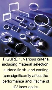
Modern excimer laser systems used in applications such as laser-assisted in situ keratomileusis (LASIK) and semiconductor microlithography demand high-performance optics and thin-film coatings. "Industrial-strength" optics designed for these systems must endure millions or even billions of intense UV laser pulses without damage. Manufacturers of high-performance thin-film coatings for industrial laser applications must examine a host of factors in the quest for high performance and long lifetimes (see Fig. 1). Substrate materials and polish, thin-film design, and accurate metrology all play an important role in achieving industrial qualification.
Substrate material selection
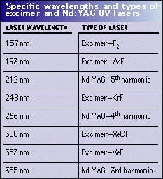
When specifying an optical component for a laser application, an early consideration should be the selection of an appropriate substrate material, which depends on the type of laser (see table). Optical components can be classified into three basic groups: cavity optics such as total reflectors and output couplers; external UV-transmitting optics, such as lenses and beamsplitters; and external non-transmitting UV optics, such as front-surface beam-turning mirrors.Excimer-laser cavity optics typically are manufactured from high-purity magnesium fluoride (MgF2) or calcium fluoride (CaF2), as these offer resistance against fluorine damage from the cavity gases. Materials such as fused silica can degrade and become etched when exposed to an environment containing fluorine gas, so they typically are not selected for use as cavity optics.
Transmitting components at 157 nm, such as beamsplitters and lenses, normally require CaF2 or MgF2 substrates. While MgF2 offers high transmission at 157 nm, it is birefringent, making it unsuitable for lithography exposure systems. Thus, CaF2 is the material of choice. Fluorine-doped "dry fused silica" is in the development stage and offers promise for components used in lithography systems because it has a lower thermal-expansion coefficient than CaF2, and thus less optical distortion. It may also find use in projection lens assemblies as a chromatic-correction material. At 193 nm and above, transmitting components can be manufactured from UV-grade fused silica, CaF2, or MgF2.
Front surface mirrors designed for use at 157 nm have been manufactured from fused silica and CaF2 substrates, although the latter has become the recommended substrate material. Fused silica can compact, crack, or craze when exposed to even small amounts of energetic 157-nm radiation.1 Front surface mirrors for 193 nm and above are routinely manufactured from UV-grade fused silica, although Zerodur, BK-7, and fine-annealed Pyrex also have been used.
Materials are available in a variety of different grades. The internal defects and trace impurities can be different with each bulk material type and grade. Therefore, in addition to selecting the best material for an application, the proper grade of that material also must be considered. Impurities and defects can contribute to absorption and scatter, fluorescence, or color centers in UV-laser-based systems.
Polish considerations
Surface figure and finish are specifications that define the quality of a polished surface. The surface figure is a measurement of the deviation from the ideal surface, in terms of peak-to-valley waves. Most UV laser optics typically are specified with a surface figure of 1/10 wave or better at 633 nm.
The surface finish of a substrate indicates the number and size of scratches and digs in a polished surface. In some applications, especially those sensitive to scatter, surface finish can be as critical as the substrate material selection. Surface finish of excimer optics is most often specified as a two number code, the first number indicating the scratch width in units of 0.001 mm, the second indicating the diameter of a dig in units of 0.01 mm. A surface finish of at least 20 to 10 scratch-dig is normally recommended for most UV laser components.
Although significant advances in polishing equipment have been made, surface preparation continues to rely on a vendor's polishing knowledge and experience. Polishing vendors have specialties based on material type, surface-finish, and optical design. Very few vendors excel in all types of optical surface preparation. Calcium fluoride is softer than fused silica and consequently special handling is required. Only a limited number of vendors have the experience necessary to polish this material economically. Surface figures of 1/20 wave or better are possible with CaF2, with correct polishing techniques.
Optical thin-film coatings
Some of the first commercially available optical coatings for UV wavelengths were Al+MgF2 designs. A typical Al+MgF2 coating absorbs approximately 10% to 14% of UV light but offers excellent broadband UV/visible reflectance, making it well-suited for multigas cavity mirrors, spectroscopy, and research applications. The development of high-power UV lasers, however, created the demand for more robust coatings. In 1973, Acton Research Corp. developed the first UV multilayer dielectric coatings, now the mainstay of high-powered laser applications. Researchers used these high-efficiency, low-loss mirrors in early laser development efforts.
Coating designs are continually improved to meet the needs of individual laser applications. Deep-UV microlithography applications, for example, utilize excimer lasers with low to medium fluence and high repetition rates. This contrasts with challenging medical applications, such as LASIK, which typically uses medium to high laser fluences with lower repetition rates. Coating designs are optimized to address specific customer requirements for long lifetimes under high fluence or high repetition rates. Independent laser testing has shown that new enhanced coatings for 193 nm can survive up to ten times longer than conventional laser coatings. Lifetime gains with new coating designs exceed 7 billion pulses, at an energy density of 20 to 40 mJ/cm2 and a 400-Hz pulse repetition rate. When used under medium- to high-power irradiation, enhanced 193-nm coatings can exceed 1,000,000 pulses at an energy density of 225 mJ/cm2 at 100 Hz.
Metrology
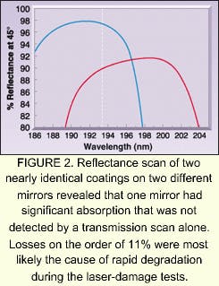
It is important to determine both the reflection and transmission characteristics of a coating to evaluate the amount of absorption at the laser wavelength, especially during the development phase of a new design. A measurement of transmission alone is not sufficient to determine the amount of absorption losses (see Fig. 2).For example, a 193-nm beam-turning mirror showed transmission of about 0.1%; however, reflectance was only 89%. Accordingly, the total absorption was about 11%. This component failed almost immediately when exposed to laser radiation. In comparison, an enhanced coating that measured nearly the same transmission (less than 0.1%) yielded 97.5% reflection, resulting in superior laser-damage resistance.
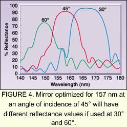
Deep-UV dielectric mirror coatings are optimized for a specific wavelength and angle of incidence. Coating performance can change dramatically depending on the angle of incidence (see Fig. 4). Dielectric mirrors have strong angular sensitivity, especially at 157 nm, where the reflecting band is narrow due to material limitations.Whenever possible, the metrology system should simulate the optical environment—be it vacuum, purged, or atmosphere. Since air absorbs light at wavelengths below 190 nm, a vacuum or purged measurement system is necessary to accurately measure coatings in this region. For optics used in a 157-nm lithography system, nitrogen-purged measurements are preferred because they simulate the environment in the exposure system.
Longer lifetimes, higher damage thresholds, and manufacturing process improvements create a powerful combination to improve performance and robustness of optical coatings, which lowers the total cost of ownership (TCO). The TCO includes not only the initial product cost, but more important, the long-term costs of replacement, downtime, and servicing. The decisions in optical design, including the factors outlined above, are critical to the TCO.
Since many initial design decisions are incorporated into final manufacturing, these decisions are critical. Many commercial laser-system providers offer service contracts; therefore the lifetime of the optics plays an import role in determining the frequency of service calls. Making the best choices will decrease TCO by lowering service cost and/or reducing downtime. It has been our experience that initial choices, some made for very valid reasons such as delivery, cost, or availability, may no longer apply as a project moves from design to production phase. Economies of scale, driven by increased production quantities, provide lower TCO opportunities that are not available at the design stage.
As new applications emerge for UV lasers, we anticipate increasing demands for higher performance and longer lifetime. Challenges facing the optics industry include design of UV optics with improved performance, superior laser-damage resistance, and lower manufacturing costs.
REFERENCE
- Massachusetts Institute of Technology Lincoln Laboratory Data (Lexington, MA).
JOSEPH McCADDEN is vice president of the optics division and LORI LABONTE is optics sales manager at Acton Research Corp., 530 Main St., Acton, MA 01720; e-mail: [email protected] and [email protected].


