Illumination spectrum affects lithographic imaging
Ivan Lalovic and Armen Kroyan
The transition from the mercury-arc lamp 365-nm line (i-line) to deep-ultraviolet (DUV) photolithographic projection imaging has presented several technological and commercial challenges to the semiconductor industry, primarily related to optical properties of the refractive imaging materials used at the exposure wavelength. Coupled with the reduction in integrated-circuit lithography size and fabrication tolerances of the critical device lithography, significant R&D and engineering have been required to achieve adequate imaging performance for volume manufacturing of sub-0.25-µm complementary metal-oxide-semiconductor and other semiconductor device technologies.
For DUV wavelengths, the choice of lens material is limited to fused silica (SiO2) and calcium fluoride (CaF2) as a result of absorbance, birefringence, and thermomechanical stability requirements. These two materials, however, exhibit significant dispersion in the DUV. Furthermore, the difference in dispersion between SiO2 and CaF2 is not large enough to allow achromatic dioptric (all-refractive) designs. Chromatic aberrations emerge due to the residual dispersion, because the law of refraction depends on the wavelength. In the image plane, the ray deviations cause dissolution of the image intensity profile and ultimately limit resolution. The degree of chromatic compensation varies depending on multiple lens-design factors (numerical aperture, optical path length, reduction ratio, field size, and so on). It also is affected by lens material, coating, and manufacturing quality.
Because the refractive-lens material dispersion in the DUV is severe, excimer laser sources with high-power spectral densities have been developed for this application. Current excimer lasers are spectrally narrowed to subpicometer levels. The spectral power trend is approaching 50 W/pm and the increase is expected to continue to enable higher optical throughput and enhanced imaging performance for next-generation lens designs. Over the last decade, the integration of krypton fluoride (248-nm) and argon fluoride (193-nm) excimer lasers has reached maturity.
Chromatic aberrations
The reduced imaging tolerances in lithographic exposure systems require optimization of all imaging parameters. The impact of the spectral width of excimer lasers and interaction with the lens aberrations cannot be ignored. Optical aberrations are broadly defined as the deviation of the real behavior of an imaging system from its ideal behavior. The deviation of the imaging system refers to phase errors of the projected wavefront. In the pupil plane, the phase error is commonly described by a nonterminating polynomial set expressed in polar coordinates, called Zernike polynomials. For practical reasons, this set is terminated at 28 or 36 terms, since only the lowest terms (the first 10 to 15) have the most direct impact on lithographic imaging of typical device patterns.
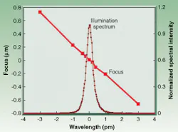
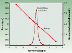
Due to material dispersion, objective-lens aberrations change as a function of wavelength. Even when line-narrowed illumination is used, therefore, characteristics of the propagating light affect lens aberrations. The variation in lens aberrations as a function of wavelength is referred to as chromatic aberration, of which a change in focus is typically the dominant effect. Tests of multiple lens systems indicate that the change in focal plane position is linear with wavelength over a wide wavelength range (see Fig. 1). A 0.15-µm focus shift was reported for a 1-pm shift in the illumination-spectrum central wavelength for a DUV lens with a numerical aperture (NA) of 0.42.1 Today's projection lenses, with NAs above 0.7, have slopes close to twice this amount.
The focus Zernike coefficient (Z3) can be computed from the shift of the focal plane Dd. Since the empirical longitudinal chromatic aberration (wavelength-defocus response) slope is known, the change of the Z3 coefficient as a function of wavelength can be calculated as follows:
null
where ÿ0 is the central wavelength of the illumination spectrum and Dd is the wavelength shift from the central wavelength.
Changes in other Zernike aberration terms as a function of illumination wavelength have been measured.2, 3 Typically, chromatic aberrations diminish for high-order Zernike terms. Nevertheless, all of the aberration-wavelength changes cumulatively contribute to blurring of the projected image.
Bandwidth and aerial image formation
Production excimer lasers for microlithography have onboard diagnostics that provide high-precision measurement of the laser's bandwidth at its full-width half-maximum (FWHM). This metric describes the width of the laser spectrum at half spectral intensity, but it does not describe the full spectral form or shape. The spectral width can also be expressed in terms of the width of the 95% energy integral. Here, the width of a larger part of the spectrum is computed; however, spectrophotometry resolution and detection noise levels for subpicometer widths present practical limitations. The spectral metrology of excimer sources is critical for establishing the understanding of the interactions between the source spectrum and lithographic process parameters.
The photolithography process involves transfer of an optically projected pattern into a photosensitive resist material. The intensity distribution of the projected image is commonly referred to as an aerial image (see Fig. 2). Image quality and resolution are influenced by various optical and mechanical parameters such as lithography geometry, numerical aperture, illumination condition, aberrations, vibration, and flare. The contrast, image log slope, and threshold width of the aerial image are used to evaluate changes of image parameters and provide input to a modeled photoresist response.
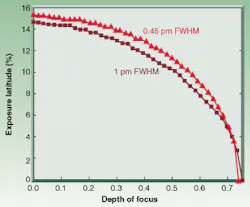
The illumination bandwidth also has an impact on image quality. The laser spectrum shape affects the aerial image through the interaction of the source spectrum and chromatic aberration response. The aerial image can be computed as a weighted superposition of images created by discrete wavelengths within a spectral range of interest; the weighting function is the spectral intensity distribution of the laser spectrum. Assuming incoherent image interactions, this effect is accurately modeled using commercial lithography simulation software.4 Using such a model, it has been demonstrated that even narrow laser bandwidths affect the aerial image properties.5, 6 The improvement in image response diminishes when bandwidth is reduced past the specification limits.
Process implications
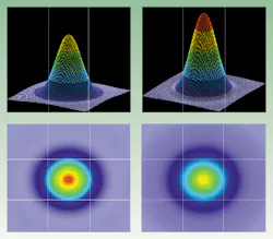
In the lithographic process, the projected aerial image interacts with multiple thin films and device surface topography to form a latent image in photoresist. The latent image is the imprint of the aerial image within the chemistry of the photoresist. A gradient of photoactivated compound is generated, which exhibits different dissolution rates when exposed to a developer solvent. When the developer is applied, photoresist patterns form. The transfer of the aerial image into a photoresist pattern is highly nonlinear and tends to approach an energy-threshold response. The resulting quality and reproducibility of the resist patterns, therefore, can vary significantly depending on the aerial image and other process properties. Because changes in the illumination spectrum induce changes in the aerial image, the spectrum also affects resist pattern properties and process performance (see Fig. 3).
The degree to which the process is affected by the laser bandwidth is determined by practically all imaging and photoresist process parameters and their interactions. Under the majority of production lithography requirements, however, the effect of the laser spectrum is not readily observable among other process error factors. This is a testament to the development and design effort, as well as performance and reliability, of excimer laser sources in fabrication facilities today.
Future lithographic requirements can only be satisfied through an understanding of all contributors to the overall process reproducibility error. Even though immediate process improvements are achieved by overcoming the most significant obstacles, a concerted industry effort is required to address the future challenges on all fronts in lithographyincluding materials, lens systems, light sources, photoresists, reticles, motion control, and contamination. Continued semiconductor-device scaling can only be realized through extensive and collaborative investigation of all error sources and interaction effects in both the lithography process and equipment technologies.
REFERENCES
- P. Yan et al., Proc. SPIE 1674, 316 (1992).
- I. Lalovic
IVAN LALOVIC and ARMEN KROYAN are lithography applications project managers at Cymer Inc., 16750 Via Del Campo Court, San Diego, CA 92127; e-mails: [email protected] and [email protected]. FIGURE 1. Measured defocus is linearly related to wavelength for a representative 248-nm krypton fluoride exposure system with a 0.6-NA projection lens. The experimentally obtained longitudinal chromatic aberration slope is 0.23 µm/pm. A typical illumination spectrum of a line-narrowed krypton fluoride laser source is also shown.


