NOVEL MATERIALS: Synthetic diamond offers much more than heat sinking
In heat-sinking applications for optoelectronic components, synthetic diamond dissipates heat much better than conventional materials such as copper and silicon carbide, enabling semiconductor-device manufacturers to produce smaller, faster, and higher-power optoelectronic devices such as laser diodes with longer lifespans and improved reliability. In fact, Element Six (Santa Clara, CA) fabricates materials with thermal conductivity ranging from 1000 to 2000 W/mK—as much as a factor of five better than copper.
But diamond is much more than a heat spreader: tightly controlled growth conditions are enabling the use of diamond as a high-power optical window, a broadband optical prism for spectroscopy, and even in detection of the Higgs boson, or the so-called “God particle.”
“Element Six grows both single-crystal and polycrystalline synthetic diamond material from a hydrocarbon-gas mixture using a proprietary microwave chemical-vapor-deposition [CVD] process,” says Henk de Wit, optical business manager for Element Six. “We eliminate chemical impurities and engineer various properties into the diamond material for predictable behavior tailored to meet the needs of a specific application. Heating a gas mixture to > 2000°C within the microwave CVD process means that high-quality polycrystalline and single-crystal materials can be produced.”
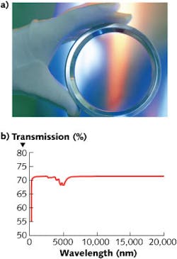
In February 2013, Element Six expanded its Silicon Valley facility to increase volume production of synthetic diamond optical windows—a critical component of laser-produced-plasma (LPP) extreme ultraviolet (EUV) lithography systems—by 50%. The process allows fabrication of high-purity diamond wafers in diameters up to 135 mm (see figure).
Diamond windows
The unrivaled room-temperature thermal conductivity of synthetic diamond makes it the perfect optical window material for high-power carbon-dioxide (CO2) lasers above 6 kW; in fact, synthetic diamond is the only material that can withstand power levels beyond 8 kW (and up to more than 35 kW). The minimal wavefront distortion of λ/20 at 633 nm enables diamond window use for EUV lithography systems. Compared to zinc selenide (ZnSe), heat generated through the absorption of light is instantly dispersed by diamond’s high conductivity into the environment to prevent the appearance of hot spots, meaning there is no need to compensate for thermal lensing.
Spectroscopy prisms
All major manufacturers of Fourier transform infrared (FTIR) spectrometers feature a synthetic-diamond-based sample holder in their product offering. Mounted CVD single-crystal diamond attenuated-total-reflection (ATR) prisms have the widest transmission spectrum of any optical material—from 220 nm to greater than 50 μm—and so improve measurement sensitivity, analysis range, and efficiency. The broadband transmission spectrum allows spectrometer manufacturers to build miniaturized devices with less-complex optical systems. Plus, synthetic diamond is scratch-resistant and both chemically and biologically inert, allowing CVD diamond spectroscopy instruments to operate in harsh, rugged environments where units with conventional prisms fail.
Particle detection
Element Six’s highest purity CVD synthetic diamond was an integral part of the CERN Large Hadron Collider (LHC) Compact Muon Solenoid (CMS) experiment and ATLAS Beam Condition Monitoring Systems used in recent experiments that revealed the discovery of a new particle consistent with the Higgs boson. Synthetic diamond was shown to be the most robust sensor material available that could withstand the harsh, high-radiation environment and react almost instantaneously to protect the advanced measurement systems. In this application, synthetic diamond was used as a sensor as part of the safety detection systems.
“The CMS experiment relies on the stability of the synthetic diamond sensors produced by Element Six to monitor the LHC beam arriving to the CMS experiment and the particles created in the collision. The robustness of this synthetic diamond-based system is crucial in protecting the most sensitive components of the 66 million channel pixel-tracking detector,” said Anna Dabrowski, CERN scientist at the CMS experiment.
About the Author

Gail Overton
Senior Editor (2004-2020)
Gail has more than 30 years of engineering, marketing, product management, and editorial experience in the photonics and optical communications industry. Before joining the staff at Laser Focus World in 2004, she held many product management and product marketing roles in the fiber-optics industry, most notably at Hughes (El Segundo, CA), GTE Labs (Waltham, MA), Corning (Corning, NY), Photon Kinetics (Beaverton, OR), and Newport Corporation (Irvine, CA). During her marketing career, Gail published articles in WDM Solutions and Sensors magazine and traveled internationally to conduct product and sales training. Gail received her BS degree in physics, with an emphasis in optics, from San Diego State University in San Diego, CA in May 1986.
