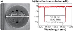
In addition to the requirement for high-speed operation and low power consumption, components for next-generation integrated, silicon-photonics-based telecommunications and computing architectures must be compact. Microdisk modulators as small as 3.5 μm in diameter have been fabricated using a depletion-based vertical p-n junction and interior electrical contacts that operate at 12.5 Gbit/s with a 3.2 dB extinction rate at 1 V drive voltage and 3 fJ/bit power consumption, but higher-order spatial modes corrupt free spectral range (FSR). This limits values to around 4 THz and consequently limits communications bandwidth. Scientists at the Massachusetts Institute of Technology (MIT; Cambridge, MA) and Sandia National Laboratories (Albuquerque, NM) have developed an “adiabatic” silicon microring modulator that maintains high speed with low power consumption at a 4 μm diameter with a 6.9 THz FSR.
In thermodynamics, the term adiabatic refers to any process without gain or loss of heat. But in guided-wave optics, adiabatic describes a structure that does not induce radiation, or otherwise enables lossless evolutions in the structure geometry. The adiabatic microring modulator design uses a narrower width in the singlemode coupling region of the ring that supports only fundamental singlemode operation without requiring a ridge waveguide. The design reduces diameter by more than 2X, doubles the FSR, and occupies 1/10 the area of comparable modulators as electrical contacts are contained entirely within the interior of the microring. Contact Michael Watts at [email protected].

Gail Overton | Senior Editor (2004-2020)
Gail has more than 30 years of engineering, marketing, product management, and editorial experience in the photonics and optical communications industry. Before joining the staff at Laser Focus World in 2004, she held many product management and product marketing roles in the fiber-optics industry, most notably at Hughes (El Segundo, CA), GTE Labs (Waltham, MA), Corning (Corning, NY), Photon Kinetics (Beaverton, OR), and Newport Corporation (Irvine, CA). During her marketing career, Gail published articles in WDM Solutions and Sensors magazine and traveled internationally to conduct product and sales training. Gail received her BS degree in physics, with an emphasis in optics, from San Diego State University in San Diego, CA in May 1986.
