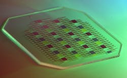
Reynard photolithography service achieves 5 µm geometries with thin-film transparent conductive materials

Reynard Corporation (San Clemente, CA) has unveiled its own custom photolithography services to manufacture patterned optics. Using a contact-exposing technique, geometries as small as 5 µm are achieved using a variety of thin-film coating materials, according to Reynard. Metallic or dielectric materials can be selected based on the application's transparent, reflective, and conductive opto-electrical requirements. Patterns can be applied to most substrate materials, including plastic sheeting.
Patterned optics are used in many markets and applications. These include elimination of electromagnetic interference (EMI) for sensitive electro-optical systems, in which the coating material is a conductive metal. The size and spacing is designed for maximum protection at a specified frequency band while providing high transmission in the visible spectrum. This design approach is used in the manufacture of high-performance aircraft windows, for example.
Another use of patterned optics is in heated windows to reduce or eliminate fogging in multi-atmospheric systems or high-humidity environments. The conductive patterns are used as heating grids that are connected to bus bars on two sides of the substrate surface. This heats the windows when exposed to low-voltage, high-current sources. This design approach is used in applications as diverse as high-altitude anti-tank missile windows and in the tips of medical endoscopes.
Wideband beamsplitters
In wideband beamsplitters that operate from UV to far IR, an evenly distributed pattern is made of many small transmission holes or blocking dots to split the energy of the radiating source. An even split of energy is achieved when the density of the transmitted region matches the density of the blocked region. The split in energy can be changed by changing the ratio of the transmission region to the density of the blocking region.
Other applications include encoder disks, liquid-crystal displays (LCDs), bar codes, reticles, transducers, and precision reference targets.
"Combining advanced thin-film optical coatings with precision photolithography patterns allows for the creation of novel optical solutions," said Forrest Reynard, president of Reynard Corporation. "It also reduces the number of optical elements in a system, which saves in system space and cost."
Substrates to 18 in. diameter can currently be accommodated, says Reynard.
For more info, see: http://www.reynardcorp.com
Source: Reynard Corp.

John Wallace | Senior Technical Editor (1998-2022)
John Wallace was with Laser Focus World for nearly 25 years, retiring in late June 2022. He obtained a bachelor's degree in mechanical engineering and physics at Rutgers University and a master's in optical engineering at the University of Rochester. Before becoming an editor, John worked as an engineer at RCA, Exxon, Eastman Kodak, and GCA Corporation.