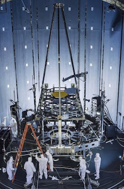
Inside NASA's Johnson Space Center (Houston, TX) giant thermal vacuum chamber, called Chamber A, the Pathfinder backplane test model of the James Webb Space Telescope (JWST) is being prepared for its cryogenic test. Previously used for manned spaceflight missions, this historic chamber is now filled with engineers and technicians preparing for a crucial JWST test.
RELATED ARTICLE: Dynamic interferometry ensures quality of large telescope optics
"The optical test equipment was developed and installed in the chamber by Exelis," said Thomas Scorse, Exelis JWST program manager. "The Pathfinder telescope gives us our first opportunity for an end-to-end checkout of our equipment."
"This will be the first time on the program that we will be aligning two primary mirror segments together," said Lee Feinberg, NASA Optical Telescope Element manager. "In the past, we have always tested one mirror at a time but this time we will use a single test system (http://www.laserfocusworld.com/articles/2011/12/jwst-undergoes-cryotest-of-all-flight-mirrors-and-passes.html) and align both mirrors to it as though they are a single monolithic mirror."
The James Webb Space Telescope is the scientific successor to NASA's Hubble Space Telescope. It will be the most powerful space telescope ever built. Webb is an international project led by NASA with its partners, the European Space Agency and the Canadian Space Agency.
SOURCE: NASA; http://www.nasa.gov/image-feature/goddard/building-hubbles-successor-crucial-pathfinder-test-set-up-inside-chamber-a

Gail Overton | Senior Editor (2004-2020)
Gail has more than 30 years of engineering, marketing, product management, and editorial experience in the photonics and optical communications industry. Before joining the staff at Laser Focus World in 2004, she held many product management and product marketing roles in the fiber-optics industry, most notably at Hughes (El Segundo, CA), GTE Labs (Waltham, MA), Corning (Corning, NY), Photon Kinetics (Beaverton, OR), and Newport Corporation (Irvine, CA). During her marketing career, Gail published articles in WDM Solutions and Sensors magazine and traveled internationally to conduct product and sales training. Gail received her BS degree in physics, with an emphasis in optics, from San Diego State University in San Diego, CA in May 1986.
