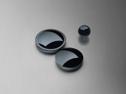
To advance their infrared glass molding capabilities, Edmund Optics (Barrington, NJ) and Fisba Optik (St. Gallen, Switzerland) have partnered in a venture that combines Fisba's process engineering and production technologies in glass molding with Edmund Optics' broad-based optical component, sales, and manufacturing expertise. The two companies aim to extend quality mass production of molded optics into nontraditional materials, specifically for IR lenses.
The investment will occur at Fisba LLC (Tucson AZ), a subsidiary of Fisba Optik. It will increase the availability of new IR optics in Edmund Optics' standard product line and for customer projects in OEM-applications by either partner. These new IR optical components are suited for life science applications such as thermal imaging and laser surgery, and for industrial and environmental applications in remote sensing and thermal imaging for detection and security.
Related article: Molded glass aspheres boost optical-design choices, by Andreas Kunz at Fisba Optik
Source: Edmund Optics

Conard Holton
Conard Holton has 25 years of science and technology editing and writing experience. He was formerly a staff member and consultant for government agencies such as the New York State Energy Research and Development Authority and the International Atomic Energy Agency, and engineering companies such as Bechtel. He joined Laser Focus World in 1997 as senior editor, becoming editor in chief of WDM Solutions, which he founded in 1999. In 2003 he joined Vision Systems Design as editor in chief, while continuing as contributing editor at Laser Focus World. Conard became editor in chief of Laser Focus World in August 2011, a role in which he served through August 2018. He then served as Editor at Large for Laser Focus World and Co-Chair of the Lasers & Photonics Marketplace Seminar from August 2018 through January 2022. He received his B.A. from the University of Pennsylvania, with additional studies at the Colorado School of Mines and Medill School of Journalism at Northwestern University.