The fin-shaped optical waveguide: for integrated photonics, this makes perfect sense
The ability of an integrated-photonics optical waveguide to confine light is ordinarily created by building the waveguide atop a continuous layer of low-refractive-index material, allowing the waveguide to channel light via total internal reflection. For example, in silicon photonics, a continuous layer of silicon dioxide (SiO2) is ordinarily placed underneath the network of silicon waveguides to allow them to function.
However, in silicon photonics, the fact that the low-index layer is continuous creates problems for the integration of photonics with electronics. In other types of integrated photonics, such as those based on III-V semiconductors, silicon carbide (SiC), or diamond, the required buried layer of low-index material weakens the structure and complicates fabrication.
Strength and simplicity
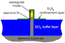
To solve this problem, Richard Grote and Lee Bassett, researchers at the Quantum Engineering Laboratory, Department of Electrical and Systems Engineering, University of Pennsylvania (Philadelphia, PA), have come up with a waveguide geometry that simultaneously allows confinement of light and a physical connection with the substrate of the same material (see figure).1
The fin is spanned by a low-index material in its lower portion and a higher-index material at its top, creating an effective index high-enough to carry light at the top, but not in the lower portions. And the all-important physical connection to the substrate is maintained.
For silicon photonics, the structure is compatible with CMOS-compatible co-integration of the silicon photonic components with VLSI (very large scale integration) electronics such as those used in computer chips. For other types of integrated photonics, the arrangement provides strength and simplicity.
REFERENCE:
1. Richard R. Grote and Lee C. Bassett, arXiv:1601.01239v1 [physics.optics] 6 January, 2016.

John Wallace | Senior Technical Editor (1998-2022)
John Wallace was with Laser Focus World for nearly 25 years, retiring in late June 2022. He obtained a bachelor's degree in mechanical engineering and physics at Rutgers University and a master's in optical engineering at the University of Rochester. Before becoming an editor, John worked as an engineer at RCA, Exxon, Eastman Kodak, and GCA Corporation.
