ZENGBO WANG and LIN LI
Galileo Galilei invented an optical microscope in 1609. He developed an “occhiolino” or a compound microscope with a convex and a concave lens. Although Galileo was probably not the first inventor of a microscope, his invention became a commonly used and powerful scientific tool—no doubt among the most important scientific achievements in the history of mankind. In 1873, Ernst Abbe established the resolution limit of optical microscopes: The minimum distance, d, between two structural elements to be imaged as two objects instead of one is given by d = λ/(2NA), where λ is the wavelength of light and NA is the numerical aperture of the objective lens. The physical origin for this limited resolution is related to diffraction and the loss of evanescent waves in the far field that carry high-spatial-frequency subwavelength information of an object and decay exponentially with distance.
For about one hundred years, the Abbe criterion was considered the fundamental limit of optical microscope resolution. But the development of near-field scanning or scanning near-field optical microscopy (NSOM or SNOM) in the 1970s to 80s, whose initial concept was proposed by E.H. Synge in 1928, was an important step in optical microscopy.1 Here, resolution of the image is limited by the size of the detector aperture instead of the illuminating light wavelength. The NSOM/SNOM has resolution of a few tens of nanometers but is practically limited by the low transmission efficiency of a small aperture and the long time to scan over a large sample area for high-resolution imaging.
Since the late 1990s, stimulated by the surge of nanophotonics, plasmonics, and metamaterials, research on super-resolution optical microscopy—optical nanoscopy—has grown rapidly. Optical nanoscopes based on Pendry-Veselago plasmonic metamaterial superlenses, nanoscale solid-immersion lenses, and nonlinear fluorescence nanoscopy have been successfully demonstrated.2–4 These techniques, however, are technically sophisticated and currently limited to narrowband wavelengths, making it difficult to achieve super-resolution capability with white-light sources in standard optical microscopes.
The microsphere nanoscope
As the name suggests, the microsphere nanoscope is based on microspheres made from ordinary materials such as silicon dioxide (SiO2) and polystyrene. It is well known that transparent microspheres can generate “photonic nanojets” with super-resolution foci, features that have been used for laser surface nanoprocessing (patterning, modification) by several groups in the past decade. For example, by combining an angular-scanning laser beam with a 1.0-µm-diameter SiO2 microsphere array deposited on a substrate, we have demonstrated near-field laser parallel nanofabrication of arbitrary-shaped patterns with 80 nm resolution.5 This has motivated us to work on optical nanoimaging with microspheres in collaborations with Minghui Hong from the National University of Singapore and professor Boris Luk’yanchuk from the Data Storage Institute (also in Singapore).
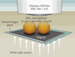
In a specific white-light microsphere nanoscopy setup, the microspheres are placed on top of the object’s surface by self-assembly. The as-received SiO2 microsphere suspension (from Bangs Laboratories in Fishers, IN) is diluted and applied to the imaging samples by drop or dip coating and the samples are left to dry in air.6 A halogen lamp with a peak wavelength of 600 nm is used as the white-light illumination source (see Fig. 1). The microspheres function as superlenses—microsphere superlenses—that collect the underlying near-field object information and magnify it (forming virtual images that keep the same orientation as the objects in the far-field) before it is projected to an 80X Olympus (Essex, England) objective lens (NA = 0.9, model MDPlan) of an Olympus microscope (model MX-850). The combination of microsphere superlenses and the objective lens forms a compound-imaging lens system. In the reflection mode, the white-light source will be incident from the top, opposite to the light source at the bottom in the transmission mode.7
The imaging mechanism
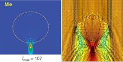
The resolution and magnification of the microspheres are fundamentally related to their focus properties and unusual light-bending capabilities (see Fig. 2). Super-resolution foci are the key requirement of microsphere nanoscopes—but not the sole factor to determine imaging resolution. Light-bending strength is another important factor affecting the magnification: Virtual images—light rays from a point source that contacts the plane of the particle—can be strongly bent toward the particle and are projected into the objective lens. The foci size and light-bending strength of the microspheres are a function of a narrow window of (n, q) parameters, where n is the refractive index of the sphere and q is the size parameter defined as q = 2πa/λ according to Mie theory.Our theoretical calculations based on Mie theory show that, for SiO2 microspheres (n = 1.46), the best particle sizes (diameters) to achieve ultrahigh-resolution imaging are between 2 and 9 µm, in agreement with the experiments.
Imaging sub-diffraction-limited objects
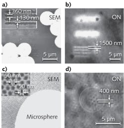
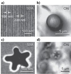
Our group has captured clear images of sub-diffraction-limited features of nanoscale objects using a microsphere nanoscope in either transmission or reflection mode. For example, 30-nm-thick chrome-film diffraction gratings with 360-nm-wide lines spaced 130 nm apart on fused silica substrates were imaged in transmission mode (see Fig. 3). The virtual image plane was 2.5 µm beneath the substrate surface, and only those lines with microsphere particles on top of them were resolved. The lines without the particles mix together and form a bright spot that cannot be directly resolved by the optical microscope because of the diffraction limit. For the visible wavelength 400 nm, the best diffraction-limited resolution is estimated to be 215 nm in air using the vector theory of Richards and Wolf, and 152 nm when taking the solid-immersion effect of a particle into account. For the main peak of a white-light source at 600 nm, the limits are 333 nm in air and 228 nm with solid-immersion effect, respectively. Here, one should also note that the focal planes for the lines with and without particles on top are different.Microsphere superlens imaging can also be accomplished in the reflection mode using halogen light illumination; in fact, the sub-diffraction-limited lines in a Blu-ray DVD disk (200-nm-wide lines with 100 nm separation) are clearly imaged with 4.74-μm-diameter microspheres (see Fig. 4). The microsphere superlens can also discern the shape of a star structure made on an antimony-tellurium (SbTe) DVD disk. The complex shape of the star, including its 90-nm-diameter corners, was clearly resolved by the microsphere superlens in reflection mode.
REFERENCES
1. E.H. Synge, Philosoph. Mag. Series, 7, 6, 35, 356–362 (1928).
2. J.B. Pendry, Phys. Rev. Lett., 85, 3966–3969 (2000).
3. J.Y. Lee et al., Nature, 460, 498–501 (2009).
4. S.W. Hell, Science, 316, 1153–1158 (2007).
5. W. Guo et al., Appl. Phys. Lett., 90, 243101 (2007).
6. G.M. Whitesides et al., Science, 295, 2418–2421 (2002).
7. Z. Wang et al., Nature Comm., 2, 218 (2011).
Zengbo Wang is a lecturer in laser micro/nanoengineering and Lin Li is a professor of laser engineering in the school of Mechanical, Aerospace and Civil Engineering (MACE) at the University of Manchester, Pariser Building, Sackville Street, Manchester, England M13 9PL; e-mail: [email protected]; www.laser.manchester.ac.uk.


