Fraunhofer ILT optical technique analyzes GaN on the nanometer scale
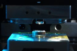
In collaboration with fellow researchers from the Chair for Experimental Physics at RWTH Aachen University (Aachen, Germany), scientists from the Fraunhofer Institute for Laser Technology (Fraunhofer ILT; also in Aachen) have developed a broadband tunable laser system based on near-field microscopy that is geared toward the particular requirements of semiconductor analysis; namely gallium nitride (GaN) and GaN composites. Wavelength can be adjusted to the material under inspection, which enables the new system to investigate a wide range of materials. The new provides the means for much faster spectroscopic analysis and has opened up access to material systems that were beyond the capacities of previous systems.
RELATED ARTICLE: GaN-on-GaN platform removes cost/performance tradeoffs in LED lighting
Using the new analysis system, the researchers in Aachen were able to obtain an optical 2D image showing tensions in the crystal structure of undoped GaN wafers for the very first time. Computer simulations helped quantify the exact extent of the tension. Recently the technique was also applied to a variety of doped GaN layers within complex structures. It’s the first time an optical technique has been available to study the structural and electronic properties of GaN and GaN composites on the nanometer scale.
Near-field microscopy offers cost and quality benefits over standard analysis techniques. The structural properties of thin GaN layers are currently studied using transmission electron microscopy; however, the costs incurred are extremely high, due in part to the laborious sample preparation process. Near-field analysis can usually be conducted without any preparation. Another benefit concerns secondary ion mass spectrometry, which is used to study the electronic properties. Although this technique can be used to determine electronic properties along an axis at the nanometer level, it isn’t yet possible to laterally ascertain the concentration of doping atoms at a comparable resolution. The technique also damages the samples. In contrast, near-field microscopy offers nanometer-scale resolution in all dimensions. It is a completely non-destructive technique and can be implemented under normal conditions.
Near-field microscopy is suitable for a range of applications. When used in close consultation with the developers of new semiconductor components, for instance, the method can help optimize process parameters in a targeted way. The analysis also aids in the understanding of physical processes from a very early stage in development, particularly at the interfaces between the individual layers. These findings can shape subsequent development stages significantly. In high-frequency and power electronics, too, GaN is becoming more and more common as a component due to its physical properties. Near-field microscopic analysis techniques are ideally suited for researching these materials.
SOURCE: Fraunhofer ILT; http://www.ilt.fraunhofer.de/en/publication-and-press/press-release/press-release-2014/press-release-2014-11-07.html
About the Author

Gail Overton
Senior Editor (2004-2020)
Gail has more than 30 years of engineering, marketing, product management, and editorial experience in the photonics and optical communications industry. Before joining the staff at Laser Focus World in 2004, she held many product management and product marketing roles in the fiber-optics industry, most notably at Hughes (El Segundo, CA), GTE Labs (Waltham, MA), Corning (Corning, NY), Photon Kinetics (Beaverton, OR), and Newport Corporation (Irvine, CA). During her marketing career, Gail published articles in WDM Solutions and Sensors magazine and traveled internationally to conduct product and sales training. Gail received her BS degree in physics, with an emphasis in optics, from San Diego State University in San Diego, CA in May 1986.
