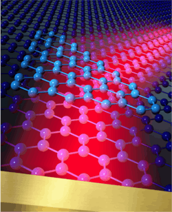
'Flatland' 2D plasmonic optics created with graphene could lead to 100X smaller integrated optics
In the interests of combining optics with electronics on graphene to develop integrated optical/plasmonic circuits, a team of Spanish and Argentinian researchers has come up with a way to fabricate fully functional 2D optics on graphene. The "flatland" plasmonic optics, which are based on resonant optical antennas and conducting patters, allow the researchers to launch and focus IR plasmons propagating along the graphene sheet.
Altogether, the experiments show that the fundamental and most-important principles of conventional optics also apply for graphene plasmons (constricted light propagating along graphene's one-atom-thick layer of carbon atoms). Future developments based on these results could lead to extremely miniaturized optical circuits (10 to 100 times smaller than conventional integrated optics) and devices that could be useful for sensing and computing, among other applications.
The researchers hail from CIC nanoGUNE and Graphenea SA (both in Donostia-San Sebastián, Spain), the Basque Foundation for Science (IKERBASQUE; Bilbao, Spain), I.N.T.I.-CONICET and ECyT-UNSAM (Buenos Aires, Argentina), and ICFO-Institut de Ciéncies Fotoniques (Barcelona, Spain).
Antenna converts light to plasmons
The technology is based on the antenna concept ubiquitous in radio-wave technology. The team showed that a nanoscale metal rod on graphene (acting as the optical antenna) can capture IR light and convert it to graphene plasmons in the same way that a radio antenna converts radio waves into electromagnetic waves in a metal cable.
"The excitation of graphene plasmons is purely optical, the device is compact, and the phase and wavefronts of the graphene plasmons can be directly controlled by geometrically tailoring the antennas," says Pablo Alonso-González, who performed the experiments at nanoGUNE. "This is essential to develop applications based on focusing and guiding of light."
The research team also performed theoretical studies. Alexey Nikitin, Ikerbasque Research Fellow at nanoGUNE, performed the calculations. "According to theory, the operation of our device is very efficient, and all its future technological applications will essentially depend upon fabrication limitations and quality of graphene," he says.
Based on Nikitin's calculations, nanoGUNE's Nanodevices group fabricated gold nanoantennas on graphene provided by Graphenea. The Nanooptics group then used the Neaspec near-field microscope to image how IR graphene plasmons are launched and propagate along the graphene layer. The researchers saw that, indeed, waves on graphene propagate away from the antenna in a standard wavelike manner.
Double graphene layers refract plasmons
To test whether the two-dimensional propagation of light waves along a one-atom-thick carbon layer follow the laws of conventional optics, the researchers tried to focus and refract the waves. A focusing experiment used a curved antenna to focus the graphene plasmons; in another experiment, a prism made of a graphene bilayer refracted the plasmons in an optical fashion.
Intriguingly, the graphene plasmons are refracted because the conductivity in the two-atom-thick prism is higher than in the surrounding one-atom-thick layer. In the future, such conductivity changes in graphene could be also generated by simple electronic means, allowing for highly efficient electric control of refraction, allowing ultrarapid steering and other manipulation of light.
Source: http://www.nanogune.eu/en/highlights/science-flatland-optics-with-graphene/
REFERENCE:
P. Alonso-González et al., Science (2014) DOI: 10.1126/science.1253202

John Wallace | Senior Technical Editor (1998-2022)
John Wallace was with Laser Focus World for nearly 25 years, retiring in late June 2022. He obtained a bachelor's degree in mechanical engineering and physics at Rutgers University and a master's in optical engineering at the University of Rochester. Before becoming an editor, John worked as an engineer at RCA, Exxon, Eastman Kodak, and GCA Corporation.
