VPIphotonics and CST partner to automate design of integrated photonic circuits
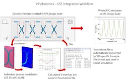
VPIphotonics (Norwood, MA) and Computer Simulation Technology (CST; Darmstadt, Germany), part of the SIMULIA brand of Dassault Systèmes, have partnered to couple full-wave photonic device simulation and overall circuit simulation and analysis of integrated photonic components and subsystems within a single framework. Highly integrated photonic circuits are on the rise, a trend expected to accelerate.
The design of complex circuits involves multiple steps, including analysis of the overall circuit simulation and performance, which requires accurate models and realistic characteristics for each embedded element. These circuit elements are typically based on information from photonics design kits (PDKs) provided by foundries. Often, full-wave photonic simulation is needed to extract accurate characteristics driving the more abstract element models on circuit-level or to study the temperature dependence of individual components being embedded in the integrated photonic circuit.
The VPIphotonics Design Suite (VPI-DS) delivers simulation of photonic circuits including purely passive, active, and hybrid subsystems and systems. The CST Studio Suite performs full-wave 3D photonic and multiphysics simulation. Linking both tools together enable engineers to combine these simulation capabilities within one single framework.
Linked both ways
If a scattering matrix does not exist for a particular element configuration, for instance, VPI-DS will automatically create ready-to-run projects that can be simulated using CST advanced solver technology, with methods including FIT/ FDTD, FEM, among others. Results from the CST Studio Suite are automatically communicated back to the waiting circuit simulation running in VPI-DS.
VPI-DS ensures that unnecessary full-wave recalculations are avoided by checking whether the characteristics of the particular element have already been calculated. Alternative case studies and various design optimizations can be executed using the VPI-DS built-in parameter sweeps and optimizations as well as a Python-based scripting environment.
VPIphotonics and CST are at OFC 2018 (13 to 15 March, 2018; San Diego, CA) in booths 4513 and 6117.
Source: VPIphotonics
About the Author
John Wallace
Senior Technical Editor (1998-2022)
John Wallace was with Laser Focus World for nearly 25 years, retiring in late June 2022. He obtained a bachelor's degree in mechanical engineering and physics at Rutgers University and a master's in optical engineering at the University of Rochester. Before becoming an editor, John worked as an engineer at RCA, Exxon, Eastman Kodak, and GCA Corporation.

