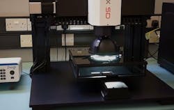
Sydor Optics obtains new objective scratch/dig measurement control capability
Sydor Optics (Rochester, NY) has announced its newest inspection-equipment acquisition, which will provide Sydor's customers with a precise and objective surface cosmetic assessment (scratch-dig) for optical component quality-control inspection. One of the strengths of this system is the assessment and application of accumulation rules which has always been a challenge for optics inspection. according to Sydor.
The Optilux SD, which is made by RedLux (Romney, UK), does this automatically using custom software assessing both scratches and digs. The software offers the additional capability to output PDF reports indicating pass/fail based on the observed defects. This new process is so accurate it may be correlated with other systems, allowing technicians to refine their production processes, or be used for secondary site verification.
The Optilux SD system automatically scans surfaces up to 300 mm square x 50 mm in thickness or multiple cavity setups while reporting all observed defects in a specified area, saving inspectors valuable time in assessing borderline defects, says Sydor.
The Optilux SD system is being tested and will be available in early fall. For system questions, contact RedLux directly: see www.redlux.net.
Source: Sydor Optics

John Wallace | Senior Technical Editor (1998-2022)
John Wallace was with Laser Focus World for nearly 25 years, retiring in late June 2022. He obtained a bachelor's degree in mechanical engineering and physics at Rutgers University and a master's in optical engineering at the University of Rochester. Before becoming an editor, John worked as an engineer at RCA, Exxon, Eastman Kodak, and GCA Corporation.
