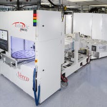
Veeco Instruments (Plainview, NY; Nasdaq: VECO) and ALLOS Semiconductors (Dresden, Germany) announced the completion of another phase of their mutual effort to provide the industry with leading gallium nitride (GaN)-on-Silicon epiwafer technology for microLED production. The purpose of the companies’ most recent collaboration was to demonstrate the reproducibility of ALLOS 200 mm GaN-on-Si epiwafer technology on the Veeco Propel MOCVD reactor system when producing epiwafers for many prominent global consumer electronics companies.
"To bring microLED technology into production, simply presenting champion values for a single metric is insufficient. It is essential to achieve the whole set of specifications for each wafer with excellent repeatability and yield," said Peo Hansson, Ph.D., senior vice president and general manager of Veeco's Compound Semiconductor business unit. "This successful joint effort reaffirms the power of combining Veeco's superior MOCVD expertise with ALLOS' GaN-on-Silicon epiwafer technology to provide customers a novel, proven and reliable approach to accelerate microLED adoption."
Sorting and binning are standard methods to achieve wavelength consistency for conventional LEDs. But microLEDs are too small and numerous to be sorted and binned; therefore, the uniformity of the epitaxial deposition is even more critical. The most important success factor for turning the promise of microLED displays into mass production reality is to achieve extremely good emission wavelength uniformity, which eliminates the need to test and sort individual microLED chips. Depending on the application and mass transfer approach, the target requirements of the industry are between +/-1 nm and +/-4 nm bin (min/max) on the epiwafer. Through this collaborative project, Veeco and ALLOS further improved the critical wavelength uniformity with the best wafer having a standard deviation of just 0.85 nm, representing an industry first on a production system.
"Veeco and ALLOS validated wafer-to-wafer reproducibility with an average wavelength standard deviation for all wafers of 1.21 nm and the peak wavelength within a +/- 0.5 nm range. With these results we made another significant leap towards the +/-1 nm bin goal on an epiwafer," said Burkhard Slischka, CEO of ALLOS. "Our technology is already available on 200 mm wafer diameter, which enables the use of low-cost and high yield silicon lines for microLED chip production. Additionally, we have a clear roadmap to enable 300 mm."
Innovators in display technology are focusing on microLED as the next significant technological shift. According to research firm Yole Développement, the market for microLED displays could potentially reach 330 million units by 2025. This optimism is fueled by the promise of microLED technology (sub-100 micrometer edge length), which is considered the critical enabler to achieving the ultimate display with much lower power consumption. However, development of such displays has been hindered by high material costs and low yield and throughput of microLED mass transfer technology. This joint technical effort effectively addresses these challenges as Veeco and ALLOS continue to work with customers to further improve GaN-on-Si epiwafer and microLED mass transfer technology.
Veeco and ALLOS will showcase details of their achievements at the International Workshop on Nitride Semiconductors (IWN) in Kanazawa, Japan on November 12, 2018.

Gail Overton | Senior Editor (2004-2020)
Gail has more than 30 years of engineering, marketing, product management, and editorial experience in the photonics and optical communications industry. Before joining the staff at Laser Focus World in 2004, she held many product management and product marketing roles in the fiber-optics industry, most notably at Hughes (El Segundo, CA), GTE Labs (Waltham, MA), Corning (Corning, NY), Photon Kinetics (Beaverton, OR), and Newport Corporation (Irvine, CA). During her marketing career, Gail published articles in WDM Solutions and Sensors magazine and traveled internationally to conduct product and sales training. Gail received her BS degree in physics, with an emphasis in optics, from San Diego State University in San Diego, CA in May 1986.
