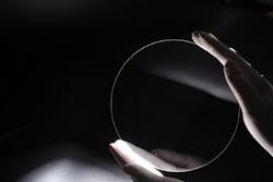
SCHOTT (Mainz, Germany) has developed optical glass wafers for augmented reality (AR) applications--branded as SCHOTT RealView--that double the total internal reflection angle compared to conventional glass wafers, enabling a larger field of view (FOV) in AR devices. SCHOTT says its RealView wafers give AR device manufacturers the first opportunity to expand the FOV almost to the limit of human peripheral vision, laying the groundwork for sizeable advances in this transformative consumer tech field.
RELATED ARTICLE: Diving into emerging AR/VR markets—opportunities for optics
SCHOTT produces raw glass in its high-tech melting facilities in Germany, and the wafer manufacturing and optical coating takes place in China, where SCHOTT recently announced a joint venture investment together with Zhejiang Crystal-Optech. "Augmented reality should still look like reality," said Rüdiger Sprengard, VP and head of Augmented Reality, Advanced Optics at SCHOTT. "To raise the bar and meet the requirements of this rapidly expanding market, manufacturers need superior optical wafers with qualities a full order of magnitude greater than what has previously appeared on the market--a challenge SCHOTT scientists and engineers have accepted in the spirit of pushing the limits of process technology and metrology."
Over the past few years, researchers at SCHOTT have leveraged their expertise in melting and surface processing of optical materials while working alongside AR technologists to understand the needs of the industry. "We have the advantage of being a fully integrated supplier, covering every step of the process to control properties that are key to the quality of the image: glass melt, wafer processing, and optical coatings," said Sprengard. "We have invested in the infrastructure to ensure we're fully capable of ramping-up production to meet demand."
SCHOTT RealView glass wafers are available with tailored refractive index and excellent light guiding properties. As a result of engineering innovation, SCHOTT RealView is 10 times flatter, measured as total thickness variation (TTV), than industry standard glass wafers.
SOURCE: SCHOTT; https://www.us.schott.com/english/news/press.html?NID=com5406

Gail Overton | Senior Editor (2004-2020)
Gail has more than 30 years of engineering, marketing, product management, and editorial experience in the photonics and optical communications industry. Before joining the staff at Laser Focus World in 2004, she held many product management and product marketing roles in the fiber-optics industry, most notably at Hughes (El Segundo, CA), GTE Labs (Waltham, MA), Corning (Corning, NY), Photon Kinetics (Beaverton, OR), and Newport Corporation (Irvine, CA). During her marketing career, Gail published articles in WDM Solutions and Sensors magazine and traveled internationally to conduct product and sales training. Gail received her BS degree in physics, with an emphasis in optics, from San Diego State University in San Diego, CA in May 1986.
