Metasurfaces enhance optical systems
The exploration of meta-optics marks a pivotal chapter in the evolution of optical technologies and presents a paradigm shift in how light is manipulated at the microscopic level. This remarkable journey from conceptual frameworks to tangible applications epitomizes the confluence of physics, materials science, and engineering, and heralds a new era of compact and efficient optical systems.
At the heart of this technological revolution are metamaterials—synthetically engineered materials endowed with unique properties unattainable in natural substances. These materials paved the way for the development of metasurfaces, two-dimensional (2D) counterparts that manipulate light at the subwavelength scale to offer unprecedented control over electromagnetic waves. This manipulation is achieved through the design of metalenses—flat lenses crafted from optical components based on metasurfaces that direct and focus light with high precision.
Metasurfaces
Metasurfaces can be active or passive. Passive metasurfaces offer fixed functionalities—serving as static elements in optical systems. In contrast, active metasurfaces represent a leap forward to tunable, reconfigurable, and time-varying functionalities. This critical innovation enables embedding multiple functions into a single layer for precise control over light’s polarization and trajectory. Consequently, bulky optical systems can now be reimagined into exceedingly small form factors, which opens the door to novel properties and applications previously deemed inaccessible with existing optical hardware.
Despite the promising capabilities of metamaterials and metasurfaces, the technology works predominantly within a narrow rather than broadband spectral operation range. Although strides are being made toward achieving broadband capabilities, challenges in efficiency, performance, and mass production persist. Nevertheless, narrowband applications are robust and driving innovation in sectors such as light detection and ranging (LiDAR) for autonomous vehicles, three-dimensional (3D) sensing, and general biometrics.
The global market for metamaterials is on an impressive growth trajectory, which is fueled by increasing applications in telecommunications, imaging, and sensing technologies. The metamaterial market size was valued at approximately $500 million in 2021 and is projected to reach over $3 billion by 2026—growing at a compound annual growth rate (CAGR) of 36%.1 This growth is attributed to metamaterials applications expanding into industries such as automotive, aerospace and defense, consumer electronics, and healthcare. Major industry players are already exploring these possibilities.
An optical revolution is underway
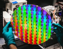
Materials engineering provider Applied Materials is redefining optical components. By creating etched waveguides and flat near-infrared (NIR) lenses on a 300 mm transparent substrate, the company showcases metamaterials in optical engineering. These components, characterized by thinness, multifunctionality, and compatibility with semiconductor nanofabrication processes, underscore significant advancements within the field. The ability to control optical elements at the nanoscale, with precise uniformity across wafers, represents a monumental leap in optical manufacturing.
Samsung Advanced Institute of Technology is at the forefront of harnessing metasurfaces for cutting-edge applications such as LiDAR—a technology crucial for autonomous driving, augmented and virtual reality, and gesture sensing. LiDAR systems, which measure distances by illuminating targets with laser light and analyzing the reflected light, are evolving. The shift toward small solid-state systems illustrates the industry’s trend toward more robust, shock-resistant solutions. Samsung’s development of a novel solid-state LiDAR system, which leverages an active metasurface based on indium tin oxide (ITO), offers enhanced scanning approaches and higher resolution at greater distances.
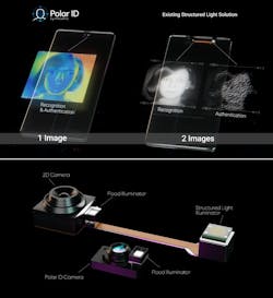
Metalenz, a spinoff from Harvard University, embodies the successful bridge from academic research to commercial viability. The company has harnessed deep-ultraviolet (DUV) lithography in semiconductor foundries to mass-produce metasurfaces with high optical yields. By collaborating with companies like ST Microelectronics and UMC, Metalenz introduced a dot pattern projector and the award-winning polarization imaging system (see Fig. 1). These innovations not only enhance 3D sensing in smartphones and IoT devices, but also introduce groundbreaking applications in biometric authentication and machine vision, which marks a significant leap toward compact, multifunctional optical solutions.
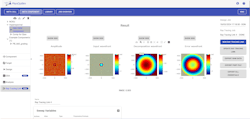
Belgium-based PlanOpSim, which was founded in 2019, makes the design and simulation of metalenses and metasurfaces more accessible and efficient. By addressing key bottlenecks such as system-level integration and area design, they came up with innovative solutions like inverse design and surrogate solvers, which significantly reduce the time and computational resources required for optimization (see Fig. 2).
Austria-based EV Group specializes in manufacturing equipment and process solutions across semiconductor and nanotechnology domains. Their expertise in nanoimprint lithography (NIL) is noteworthy, because they offer a cost-effective method to create nanometer-scale patterns essential for metamaterials and metasurfaces. EV Group’s comprehensive UV-NIL product line, capable of accommodating substrates of varying sizes, demonstrates its role in facilitating the large-scale production of these advanced materials. Through SmartNIL technology, the company enables the fabrication of nanometer-sized pillars, the basic elements of metasurfaces on a wafer scale. These are the necessary tools for the future mass production of optical components with unprecedented precision and efficiency.
California-based Synopsys, known for electronic design automation, expanded its prowess into the optical domain with a tool that represents a paradigm shift in metalens design by offering a fully automated, inverse-design capability to simplify the creation of novel metalens designs. By enabling designers of varying expertise levels to quickly generate and optimize metalenses, Synopsys is democratizing access to advanced optical components. Their software solutions not only accelerate the design cycle, but also reduce costs and physical space requirements. This facilitates the integration of metamaterials and metasurfaces into a broader array of products and technologies and paves the way for hundreds of other companies in the domain to experiment with meta-optics in their products.
The innovative terrain of meta-optics unveils a thrilling fusion of theoretical physics, engineering prowess, and visionary commercial applications. From the academic halls to the industry, this multidisciplinary endeavor has given birth to technologies that challenge the very nature of light manipulation and promise to redefine our interaction with the optical world. Whether it’s through the development of compact, high-efficiency LiDAR systems for autonomous vehicles, the creation of meta-optic components for consumer electronics, or the pioneering software solutions for the next generation of optical design, these players are at the forefront of an optical revolution.
Growth on the horizon
Market data on metamaterials and metasurfaces reveals a sector ripe with opportunities, driven by technological advancements and growing applications across multiple industries. As the market continues to expand, the ability to mass-produce metamaterial-based components at a lower cost will be crucial for wider adoption.
The surge in market growth is accompanied by significant investments from venture capital firms, government bodies, and strategic partnerships between academic institutions and industry leaders. Beyond this, research grants and funding for metamaterials projects from governmental and international bodies further fuel innovation and development in this field.
As these technologies continue to evolve, they challenge the status quo and offer a glimpse into a future where optical systems are not only more compact and efficient, but also capable of functionalities beyond the current imagination. As the field advances, overcoming the hurdles of mass production and broadband capabilities, the potential applications of meta-optics seem boundless, promising to redefine the landscape of optical technologies for years to come.
REFERENCE
1. See www.marketsandmarkets.com/Market-Reports/metamaterials-market-139795737.html.
About the Author
Ivan Nikitski
Dr. Ivan Nikitski serves as a Photonics Technology Expert at EPIC, the European Photonics Industry Consortium, which stands as the world's largest association of photonics companies with over 800 corporate members. Ivan earned his Ph.D. with honors in photonics from ICFO, the Institute of Photonic Sciences. After successfully transitioning to an expert role in the semiconductor industry in France, he now provides a special blend of academic and industrial views on integrated photonics, optoelectronics, advanced materials, and quantum technologies.


