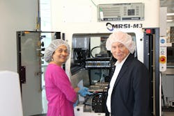
MIT kicks off FUTUR-IC to establish path to global microchip sustainability
Laser Focus World: Can you introduce us to FUTUR-IC and explain your goals?
Agarwal and Kimerling: FUTUR-IC supports continued scaling of semiconductor system performance while targeting net zero environmental impact by 2050 for the global community.
The balance between human existence and microchip benefits is being severely challenged by a relentless and unsustainable appetite for electronics consumption. For the first time in more than 40 years, the semiconductor microchip industry is confronted with limits to transistor size, its environmental footprint, and its workforce pipeline readiness.
The U.S. National Science Foundation’s (NSF) Convergence Accelerator Track I program, “Sustainable Materials for Global Challenges,” has been established under the leadership of Program Director Dr. Linda Molnar. Through Phase 2 of this program we have established a global microchip sustainability project called FUTUR-IC, which creates three-dimensional (3D) technology, ecology, and workforce research solutions to sustain the continued progress of the semiconductor manufacturing and the information systems industry. FUTUR-IC will enable companies to make multidimensional decisions based on the consequences for people, the planet, and profits.
LFW: How big of a challenge is sustainability and dealing with vast quantities of electronic waste?
Agarwal and Kimerling: Frontier constraints in the microchip industry are:
- Technology/profits. Enhanced microchip functionality for next-generation applications such as artificial intelligence (AI), 6G, light detection and ranging (LiDAR), etc. can no longer depend solely on shrinking the dimensions of a transistor.
- Ecology/planet. Net zero environmental impact for a product life cycle is critical to life on Earth.
- Workforce/people. Leadership from a new green-literate STEM workforce is required.
Concurrently engineered solutions are expected to build a common learning curve to power the next 40 years of progress for the semiconductor industry, while minimizing use of toxic chemicals, water, and minerals, and while producing less e-waste and greenhouse emissions. The plan must include ways to reduce/reuse/recycle/repair and upgrade microchip-containing systems.
LFW: Can you unpack the electronic-photonic integration part of the program for us?
Agarwal and Kimerling: The Chip-Scaling Era has ended, and Package/System-Scaling Era is now underway with no long-term technology roadmap. To maintain performance scaling, incremental technology change is insufficient, and supply chain sustainability in terms of workforce quality, materials criticality, and manufacturing effluent has no inherent scaling vector. Economic risk has never been so large, and rarely been so dependent on a particular technology evolution.
This transformation to chip/package scaling isn’t a task that any one sector can tackle in isolation; it requires a robust global alliance that unites academia, industry, government, and community. FUTUR-IC offers collective research projects and partnerships to pave the way for innovative solutions, ensuring a resilient and prosperous technological future. One such initiative involves electronic-photonic integration and co-packaging.
Technology solutions require synchronized innovation along the supply chain, from materials suppliers to system integrators to end users. FUTUR-IC supports continued scaling of system performance while targeting net zero environmental impact by 2050 for the global community.
Semiconductor hardware, software, and system architectures are undergoing simultaneous technology transitions today that present both opportunities and uncertainties. The information systems that drive data center workflows and ubiquitous sensing installations for the Internet of Things (IoT) aim to do the impossible: Scale down costs, energy consumption, and latency to nearly zero, while simultaneously amplifying bandwidth and connectivity to seemingly infinite levels, within environmental constraints.
FUTUR-IC has adopted electronic-photonic package integration as its hardware driver. It targets scaling chip package input-output (I/O) to >1 petabit/second within a net zero ecology envelope.
Investment examples are:
- PFAS-free materials and process flows to meet package scaling requirements;
- Adhesive materials database for low-temperature assembly; and
- Demonstration of new chip package architectures that mitigate end-of-life waste under a new paradigm for a circular industry, including the design for upgrade, repair, reduce, reuse, recycle (DfUR4) initiative.
LFW: What’s the coolest part of FUTUR-IC?
Agarwal and Kimerling: We were pleasantly surprised to find that so much microchip sustainability-related work has already begun using the simple ideas: Reduce, reuse, recycle, repair, or upgrade. It’s cool to see the commitment of industry and its willingness to work with FUTUR-IC to find the right solutions.
A new knowledge base to be built from a different research constituency must be brought in—a path that’s different from shrinking transistors. With the advent of AI and related applications, the influence of success on the future of society is highly leveraged compared to the past. The role of social agency in accepting new technology will be as important as creating new circular technology.
Industry organizations are eager to quickly bring innovations to be adopted by the market. With FUTUR-IC partnerships, these can serve as seeds for sustainable microchip growth of next-generation systems.
LFW: If people want to get involved in the program or support it, can they join?
Agarwal and Kimerling: Absolutely—please contact Dr. Anuradha Murthy Agarwal at [email protected].
LFW: Timeline to make things happen?
Agarwal and Kimerling: We’re open for business now. There’s an urgent need to move things along rapidly to avoid regrettable solutions for the future and provide circular solutions instead.
This is the time for disruptive freedom to make the right choices in designs, materials, processes, and systems—instead of being content with just another iteration—to obtain exponential growth of the market within ecological constraints.
