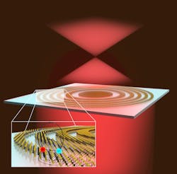
Thanks to quantum effects, a team of physicists led by Jorik van de Groep’s 2D Nanophotonics group at the University of Amsterdam managed to create a flat lens a mere three atoms (0.6 nm) thick (see video). Lenses are normally curved to refract and focus light, but the group’s approach uses concentric rings of tungsten disulfide (WS2) with gaps between them to form a Fresnel zone plate lens that focuses light via diffraction instead of refraction.
The magic comes from the size of the rings and distance between them—compared to the wavelength of light hitting it—and it determines the focal length of the lens. At the same time, the operation of the lens that focuses the light is dictated by the quantum mechanical exciton resonances of the monolayer, which allows WS2 to absorb and re-emit light at specific wavelengths.
“While electronics are miniaturized, optics are still bulky,” points out Ludovica Guarneri, a Ph.D. researcher working with van de Groep. “In fact, even the newest smartphones still have a camera sticking out of them. To solve this challenge, a new class of optical coatings—metasurfaces—were developed and a pattern of nanoscale structures collectively scatter light to perform an optical function, such as lensing in a ~100-nm-thick coating.”
New 2D quantum materials, such as monolayers of transition metal dichalcogenides (TMDs) including WS2, offer a remarkably strong and tunable light-matter interaction due to their quantum mechanical exciton resonances.
“We were intrigued by the properties of these materials and wondered whether we could leverage the excitons within this material as resonant building blocks instead of the nanostructures in established metasurfaces,” Guarneri says. “This resulted in our work, in which we set out to develop a new generation of optoelectronic metasurfaces—pushing the size down to atomic thicknesses.”
Lens design work
Fabrication of the team’s lens requires several cleanroom steps. It starts out with a high-quality, large-area monolayer of WS2 on a sapphire substrate, which is achieved via gold-assisted exfoliation. During this process, the outer atomic layer is peeled off a source crystal using a flexible tape made of gold and then transferred onto the sapphire substrate.
“Our atomically thin lens is created by directly patterning the monolayer via electron-beam lithography and reactive-ion etching,” says Guarneri. “The design is a Fresnel lens, a.k.a. zone-plate lens, optimized to focus light at a 620-nm wavelength, which is the spectral location of the strongest WS2 exciton resonance, 1 mm away from the surface.”
When the team characterized the focusing efficiency spectrum of the lens around resonance, they discovered its spectral line shape mirrors the electronic susceptibility of the material.
“The electronic susceptibility of monolayer WS2 is, in turn, governed by exciton resonance,” explains Guarneri. “To further explore the relationship between excitons and the functionality of the lens, we studied both the focusing efficiency and optical properties of the material as a function of temperature.”
It turns out, lowering the temperature directly affects the nonradiative decay rate of the exciton and it leads to an increased excitonic quantum yield. Acting on the excitons’ recombination rates “impacts the focusing efficiency of the lens, which increases as the temperature is lowered—and it proves the spectral-line shape of the focusing efficiency is dictated by the excitonic decay rates,” Guarneri says.
Biggest hurdle involved in this work? Measuring the temperature-dependent data. In fact, it required building a custom optical setup around a helium cryostat, which meant the team needed to measure the focus formed inside the cryostat by positioning an optical imaging and laser setup outside the cryostat.
“It required very careful design and alignment,” says Guarneri. Acquiring the measurements was also a delicate procedure, because they probed a tiny signal—light focused by the lens—on top of a large background (light being transmitted through the nearly transparent substrate).
“Lastly, the data analysis was quite involved and required a lot of thinking outside the box, since we wanted to carefully quantify the fraction of the incident power that was focused by the lens,” Guarneri says.
The coolest part of this work for Guarneri was the first time she saw on the camera that light was actually being focused by such a thin lens—~0.6 nm. “Next to this, it was truly fascinating to read the strong fingerprint of the excitons on the performance of the lens—its focusing efficiency spectrum,” she adds.
Anatomically thin optical metasurfaces based on exciton resonances
With this work, the physicists are paving the way to a class of anatomically thin optical metasurfaces based on exciton resonances, where light is manipulated within a single layer of atoms. The low efficiency that characterizes these elements can be used as an advantage for applications where transparency is a benefit—eyewear such as eye tracking, virtual reality (VR), and augmented reality (AR) goggles.
“In our next work, we’ll leverage the tunability of the exciton resonances within monolayer TMDs to obtain dynamic metasurfaces where the designed operation can be actively modified,” says Guarneri. “These 2D quantum materials have a refractive index that can be tuned electrically, which is a direct result of the exciton resonance.”
This tunability is unique to optical materials, which typically have a fixed refractive index. “Using this, we want to create atomically thin optical coatings that can change their optical function on demand—steer light to the left or right using electrical voltages, for example, or change the focal distance of a lens. It could have a major impact on technologies where active control over light is essential, such as AR/VR, optical communications, and LiDAR,” Guarneri says.
FURTHER READING
L. Guarneri et al., Nano Lett., 24, 21, 6240–6246 (2024); https://doi.org/10.1021/acs.nanolett.4c00694.
About the Author
Sally Cole Johnson
Editor in Chief
Sally Cole Johnson, Laser Focus World’s editor in chief, is a science and technology journalist who specializes in physics and semiconductors.


