Editor's note: Listen to our podcast interview with Todd Haugen below, which we released on February 25, 2025.
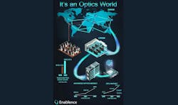
The culmination of mature optical manufacturing capabilities, Moore’s law hitting a wall, the explosion of AI growth, and the development of true optical computing capabilities are all contributing to a new wave of growth across the optics industry.
Today, the electronics industry has reached the operational limits of advancements in electronics with the advent of 4-nm technologies being rolled out by leading chip manufacturers. Moving forward, the industry is increasingly turning to optics for continued advancements in throughput and to handle latency.
The transformative role of AI optics is the driving force behind this growth within three key optics segments:
Optical communications. Optical communications typically involve fiber optics (internet, telecommunications) and the market is reaching maturity. But it’s still growing, and AI will continue to fuel its growth for the next several years.
Optical sensing. This segment focuses on the use of optics for sensing technologies. Optics were initially developed for communications, but expanded in the 1980s and 1990s to include sensing applications like medical devices, automotive light detection and ranging (LiDAR), and manufacturing. This market has grown significantly, especially within the past few years, because digital transformation and AI accelerated its adoption.
Optical computing. This is a fast-emerging area, and research during the 2000s revealed the potential for optics to break through the limitations of Moore’s law. As electronic circuitry faces physical limitations, optical computing offers a potential solution by enabling faster, more efficient processing. Companies like NVIDIA and AMD are investing heavily in optical compute R&D, particularly for AI applications.
Promise of optics chips
The promise of optics chips for compute, among other functions, is emerging as a viable technological solution to overcome traditional electronics limitations. For example, optics devices are superior in speed, energy consumption, and bandwidth while generating minimal heat. Optics processors operate efficiently at room temperature, which minimizes the need for the specialized cooling systems found in data centers using traditional central processing units (CPUs) and graphic processing units (GPUs).
As traditional semiconductor technologies (electronic chips) reach their limits, particularly with the introduction of 4-nm transistors, optical technologies are gaining traction, thanks to their advantages in speed, energy efficiency, and bandwidth. As demand for AI surges, particularly for large language models (LLMs) and other AI applications, this traction will intensify and drive major growth of optical communications and optical compute segments.
AI needs optics in four key areas
Overall network capacity. Training AI models will require vast amounts of data and computing power, which will, in turn, increase demand for high-bandwidth, low-latency optical networks.
High-bandwidth, low-latency connectivity. Data centers used for AI computations (such as large GPU clusters) require high-speed, low-latency interconnects. This is driving the growth of co-packaged optics (CPOs) and advanced NxN routers.
AI compute inside the chassis. Companies like Enablence, Lightmatter, Lumentum, and others are integrating optics directly into AI computing hardware to improve throughput while reducing power consumption and heat generation. This trend will continue.
Advanced vision systems. The growing importance of AI optics for advanced vision systems, such as LiDAR—used in autonomous vehicles, drones, robotics, and medical imaging—is also significant and will propel that market as AI matures. AI is already accelerating the adoption of these systems in industries like automotive LiDAR, aerospace, defense, and medicine. Optical technologies are helping improve capabilities like diagnosing diseases, enabling self-driving cars, and advancing robotics and drones.
Three key optics platforms
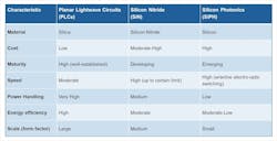
To enable these opportunities in AI, the industry is relying on three main optics platforms: planar lightwave circuits, silicon nitride, and silicon photonics (see table).
Planar lightwave circuits (PLCs). A proven and cost-effective technology with substantial benefits in terms of power handling and energy efficiency.
Silicon nitride (SiN). A developing technology with moderate to high costs.
Silicon photonics (SiPH). An emerging platform particularly suited for high-speed and low-latency applications, but at a higher cost.
Hybridized optical platforms support growth
No one platform strategy will dominate because each comes with specific advantages depending on the application and requirements. A hybridized approach will be necessary to support customer and industry needs.
Enablence Technologies will continue to specialize in manufacturing optical components using market-proven PLC technology to provide high-power handling, low-loss devices that feature efficient use of space, especially for interconnects within AI data centers and for telecommunications.
Increased growth and investment ahead
To leverage optics capabilities, the industry will need to continue to make significant investments in R&D. During the next five years, the industry will undergo a massive transformation, driven largely by AI, Moore’s law limitations, and advances in optical compute technologies.
Optics is on the cusp of significant expansion into the semiconductor realm, largely fueled by advancements in AI and the increasing limitations of traditional electronics. Recent history shows us traditional electronics experienced limitations in physics that are restricting innovation, particularly in AI.
But optics can overcome these limitations—it’s delivering 10x the throughput for memory and networking at 1/100th the power consumption and heat generation. Precision sensing modules are delivering additional dimensions of data not available through other mediums. These advantages are driving rapid growth across all optical segments and confirm that optics is the solution the market needs today.
About the Author
Todd Haugen
Todd Haugen is CEO of Enablence Technologies, a supplier of optical chips based on PLC technology serving datacom, telecom, automotive, and artificial intelligence (AI) applications.


