The rapid growth of artificial intelligence (AI) and high-performance computing (HPC) applications is driving unprecedented demand for high-bandwidth, low-latency, and energy-efficient optical interconnects for AI infrastructure.
These applications require increasingly scalable and cost-effective photonic solutions for data transfer, so silicon photonics has emerged as a key technology for transceivers and other optical interconnect functions. Major semiconductor foundries—including TowerJazz, GlobalFoundries, Intel, TSMC, Samsung, and STMicroelectronics—are maturing and marketing silicon photonics capabilities, which validates the importance of this technology as the backbone for next-generation communication and computing systems.
Laser integration challenge
Despite silicon photonics’ tremendous progress, one persistent challenge is the integration of high-performance lasers and optical gain. Some link architectures may suffice with a “remote laser” packaged separately and fiber coupled to the silicon photonics, but having on-chip optical gain is extremely beneficial when it comes to minimizing power consumption and footprint, and maximizing performance. In the pursuit of integrated optical gain, some commercially available platforms leverage flip-chip bonding of fully fabricated laser or gain chips, while others rely on bonding of wafers or chiplets followed by fabrication. These methods add complexity and cost, and are limited in scalability and achievable gain density (number of gain elements per die).
A more elegant solution is the direct epitaxial growth of laser material on silicon, which would enable integration into silicon photonics’ front-end fabrication processes. Metalorganic chemical vapor deposition (MOCVD) is emerging as the leading technique for this approach because it offers scalability and selective area growth—the ability to deposit the material selectively within patterned structures between other components. This deposition could be carried out in a similar manner to which germanium is deposited selectively for integrated photodiodes in silicon photonics.
MOCVD vs. MBE: Process integration and scalability
Historically, molecular beam epitaxy (MBE) was leveraged to synthesize group III-V compound semiconductor materials for research and development, and for low-volume production. MBE’s lower throughput and higher operational costs are barriers to large-volume manufacturing. In contrast, MOCVD has become an industry standard for large-volume manufacturing of technologies such as light-emitting diodes (LEDs), high-electron-mobility transistors (HEMTs), and vertical-cavity surface-emitting lasers (VCSELs). Beyond scalability, MOCVD affords selective area growth that enables process integration, a characteristic that may prove invaluable for silicon photonics.
Quantum dots: Ideal gain media for silicon photonics
For on-chip optical gain, quantum dots (QDs) offer compelling advantages over traditional quantum wells. QD lasers demonstrate lower threshold current, lower temperature sensitivity, and lower linewidth enhancement factor. The latter attribute makes QD lasers particularly well suited to narrow-linewidth laser and comb source applications.
Another benefit for integration with silicon photonics, QD optical gain media are less sensitive to optical back reflection, eliminating the need for optical isolators. QDs are also more tolerant of material defects because carrier migration lengths are over an order of magnitude shorter, and the discrete dots distribution provides defect trapping capabilities.
MOCVD QD lasers: Manufacturing breakthrough
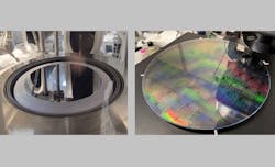
While MBE was traditionally used to create QD lasers, MOCVD would be preferred for its scalability and process integration. Aeluma is synthesizing high-quality QDs by MOCVD on 200- and 300-mm substrates—commonly used for silicon photonics—via a selective area growth method. This selective area MOCVD growth approach circumvents the challenges associated with wafer and chiplet bonding, and provides a more straightforward solution to optical gain integration that’s front-end process compatible. This monolithic integration approach also provides ultimate flexibility for engineering novel laser cavity designs and facilitates ultrahigh gain integration density.
Meet the demands of next-gen computing
The scalability of MOCVD-grown QD lasers may address the growing demand for high-bandwidth, low-latency, and energy-efficient optical interconnects for AI and HPC applications. Modern AI workloads require massive data transfer for intra- and inter-data center communications, pushing traditional electronic interconnects beyond their fundamental limits. Silicon photonics with integrated QD optical gain provides a path to scale optical interconnect technology for next-generation systems.
About the Author

Bei Shi
Bei Shi is a Principal Scientist for Aeluma, Inc., a semiconductor company based in Goleta, CA.
