Thin-film Coatings: Ultrathin tunable conducting oxide nanofilms create broadband, near-perfect absorbers
ALEKSEI ANOPCHENKO and HO WAI HOWARD LEE
Ultrathin optical films with strong absorption are required for a number of optical applications, including light-harvesting technologies and high-resolution optical space technologies. However, perfect absorption (>99.9%) usually requires multiple optical film layers with high losses and large thicknesses. Consequently, there is significant interest in the development of new ultrathin optical films with advanced functionalities. Our team at Baylor University studies conducting oxide epsilon-near-zero (ENZ) materials that can be used to make ultrathin perfect absorbers with broadband and electronically tunable responses.1
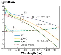
Transparent conducting oxides (TCOs) are semiconductors with high transmittance at visible and near-infrared (near-IR) frequencies, and they can be heavily doped with typical quasi-neutral-region charge carrier concentrations between 1019 and 1021 cm-3, thus exhibiting metallic characteristics (such as negative permittivity) in the visible or near-IR regime depending on the carrier concentration of the materials (see Fig. 1).2, 3
While the TCOs exhibit metallic properties, their material loss is significantly lower than noble metals such as gold and silver, giving them significant potential as alternative plasmonic/metasurface materials.4 Importantly, the carrier concentration of TCOs can be varied by different fabrication methods, deposition parameters, and post-processing techniques.
The ellipsometry measured complex permittivity (ε) of indium tin oxide (ITO) ultrathin films varies with different sputtering temperatures, for example, and materials with different ENZ (-1 < Re(ε)r < 1) frequencies and low material loss (Im (ε)I < 0.5) are routinely fabricated in our lab. The ENZ wavelength could further be adjusted to visible wavelength by higher sputtering temperature/annealing processes and electrical gating. The standard free-electron Drude model accurately describes the complex permittivity around the ENZ wavelength.
Interestingly, ENZ properties can be observed in these TCOs typically in the near-IR range. Unique properties observed in the ENZ regime include enhanced absorption in TCO films, advanced resonant coupling properties with optical antennae, and strongly enhanced nonlinear response and light generation in a TCO slab.5-7 In addition, electrical tuning of conducting oxide materials to the ENZ regime results in efficient light manipulation and modulation.8 We use this special ENZ optical region of the TCOs to develop ultrathin, tunable, and broadband perfect-absorber coatings.
ENZ-modes in TCO nanolayers
Our team has grown smooth, ultrathin (<100 nm) TCO films and multilayers such as aluminum (Al)-doped zinc oxide (ZnO) or AZO and ITO by atomic layer deposition (ALD) and radio-frequency (RF) sputtering at elevated temperatures, respectively. The ENZ frequency of the TCO nanolayers in the near-IR region is controlled by the growth temperature, chemical precursor ratios, the number of ALD monolayers, and others.
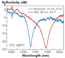
Ultrathin ENZ layers support radiative Berreman (above light line) and bound ENZ (below light line) polariton modes.9 Similar to the surface plasmon-polariton mode in metal films, the ENZ mode in TCO nanolayers may be excited in the attenuated total internal reflection or Kretschmann-Raether configuration with an incidence angle above the critical angle (see Fig. 2).The excitation of the polariton modes leads to an enhanced electric field confined within the TCO nanolayer of the thickness approximately λENZ/100 and enhanced optical local density of states and strong light absorption. The perfect absorption (or zero reflectivity and transmissivity) occurs when the wavelength, thickness, and angle values satisfy the condition for critical mode coupling.
ALD-grown AZO broadband absorber
Growth of AZO nanolayers using ALD enables fine control of their thickness and ENZ wavelength.10 It also provides a desired surface smoothness of AZO nanolayers for conformal and multilayer deposition. We designed and fabricated ALD-grown broadband ENZ absorbers with more than 90% of absorption in the near-IR by stacking AZO nanolayers with varying ENZ frequency.11 The thickness and ENZ wavelength of each AZO nanolayer are controlled by varying the number of deposition cycles and the deposition ratio of diethylzinc-H2O to trimethylaluminium-H2O.
Three AZO nanolayers, AZO1, AZO2, and AZO3, with the deposition ratio of 20:1, 35:1, and 30:1, respectively, constitute the prototypical broadband absorber. The complex permittivity of the AZO nanolayers is measured by spectroscopic ellipsometry on control samples. Zero permittivity is located at wavelengths of 1497, 1571, and 1700 nm for AZO3, AZO2, and AZO1, respectively. The absorption bandwidth of the desired broadband absorber depends on a choice of the ENZ wavelengths, thicknesses, and the number of AZO nanolayers constituting the device.
To achieve broadband absorption, we used a parametric sweep to optimize the thicknesses of the three AZO layers. At an angle of incidence of 43°, the absorption bandwidth of 214 nm for Berreman mode and 294 nm for ENZ mode are achievable for a multilayer stack with the AZO thicknesses of 80, 60, and 50 nm (for the bottom, central, and top layers, respectively).
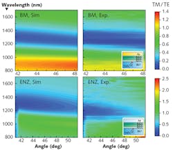
Measurements of TE and TM reflectivity spectra from the designed AZO stack in the Kretschmann-Raether configuration over a range of incidence angles from 41° to 52° show a minimum in TM reflectivity because of resonant light absorption by the ENZ modes. The measured TM/TE reflectivity ratios can be compared with the ratios of simulated reflectivities (see Fig. 3).The simulation takes into account the real thicknesses and optical properties of the constituent AZO layers of the multilayer stack measured by the ellipsometry on control samples. The comparison shows a good agreement between the measured and simulated results, which confirms a successful fabrication of the AZO broadband absorber.
Field-effect tunable perfect absorber
Perfect optical absorption—or absorption >99.9%—is achievable in TCO nanolayers with a thickness that approaches the Debye length of the accumulation layer in field-effect devices such as a metal-oxide-semiconductor (MOS) capacitor. Based on this observation, we demonstrated post-fabrication electrical tuning of the perfect absorption in a MOS-like absorber.1
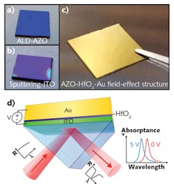
Our tunable perfect absorber structure consists of a thick (opaque) gold layer, 5-nm-thick hafnium dioxide (HfO2), and the ITO nanolayer with a thickness <10 nm (see Fig. 4). The field-effect tunable absorber supports the Berreman mode and the direct perfect absorption tuning is achieved through the formation of an electron accumulation layer at the HfO2-ITO interface upon the application of external electrical bias to the field-effect device.The study of broadband and field-effect tunable TCO ENZ thin-film absorbers is expected to advance the field of ultrathin optical films with new functionalities, enabling active manipulation of light properties with unprecedented extension to the visible/near-IR spectrum with large-dynamic-range, energy-efficient, and ultrafast tunable processes. These tunable and broadband ENZ perfect absorbers have many potential applications in nonlinear and quantum ENZ optics, thermophotovoltaics, hot-electron generation in the ENZ regime, and other fields.
REFERENCES
1. A. Anopchenko et al., ACS Photonics, 5, 7, 2631–2637 (2018).
2. G. V. Naik et al., Adv. Mater., 25, 24, 3264–3294 (2013).
3. A. Boltasseva and H. A. Atwater, Science, 331, 6015, 290–291 (2011).
4. S. Q. Li et al., ACS Nano, 5, 11, 9161–9170 (2011).
5. M. Z. Alam et al., Science, 352, 6287, 795–797 (2016).
6. J. Kim et al., Optica, 3, 3, 339 (2016).
7. Y. M. Yang et al., Nat. Photonics, 11, 6, 390–395 (2017).
8. Y. W. Huang et al., Nano Lett., 16, 9, 5319–5325 (2016).
9. S. Campione et al., Phys. Rev. B, 91, 12, 121408 (2015).
10. A. Anopchenko et al., Mater. Res. Express, 5, 1, 014012 (2018).
11. A. Anopchenko et al., OSA Technical Digest (online), paper JTh2A.94 (2017); https://doi.org/10.1364/cleo_at.2017.jTh2A.94.
Aleksei Anopchenko is postdoctoral fellow in the Department of Physics at Baylor University, Waco, TX, while Ho Wai Howard Lee is assistant professor at Baylor University and fellow at the Institute for Quantum Science and Engineering at Texas A&M University, College Station, TX; e-mail: [email protected]; www.baylor.edu.
