Silicon Photonics: Automated wafer-level probing meets silicon photonics
JOE FRANKEL, KAZUKI NEGISHI, MIKE SIMMONS, DAN RISHAVY, and ERIC CHRISTENSON
As chip designers are pressed for ever-increasing data rates, the use of wavelength-division multiplexing (WDM) with infrared photonic signals as a data transfer medium is increasingly finding its way into CMOS silicon-based devices. Termed “silicon photonics” (SiPh), this technology is not only being used to displace traditional electrical interconnects, but also for a broad range of applications, including lidar, quantum computing, and biosensing.
The integration of optical components on a chip creates a host of new challenges and demands for wafer-level probing of SiPh devices, where huge volumes of device-performance data are required to carry a design from concept to qualification and into production. While working in a lab on an initial prototype, it may suffice to spend minutes or in some cases hours to set up and align a single device for measurements. However, such time- and effort-intensive methods are unsuitable for the cycle-time demands of high-volume SiPh manufacturing.
A huge leap forward in throughput is required to quickly get process feedback and take these designs to the next level. In addition, input/output (I/O) measurements must be made with alignment precision on the order of nanometers due to the effective aperture dimensions of optical gratings and waveguides fabricated in silicon—a precision heretofore unheard of with traditional probing systems.
As device technologies evolve from simple transmission lines to optical-to-electrical converters to optical modulators and beyond, manufacturers must keep pace to produce prober platforms that enable chip designers to test and improve their rapidly maturing SiPh designs. Starting in 2017, FormFactor developed a wafer-level probing solution that supports a wide variety of SiPh applications, with a development roadmap to support the rapidly evolving SiPh industry.
Probing applications
Silicon photonics probing applications typically fall into the category of either modeling and characterization, wafer acceptance testing, or production process monitoring. Each of these application categories places its unique relative emphasis on accuracy, throughput, and test flexibility.
Modeling and characterization applications seek to extract model parameters used to design and simulate the device, or portions thereof. In this case, precision is key, but throughput is not as important since modeling is a design engineering activity.
Wafer acceptance applications seek to verify performance of the chip design, examining device functionality, repeatability, and performance of multiple devices across the substrate. In this case, a balance between precision and throughput is important so that the fabrication process can be proven over samples of many devices.
Inline process monitoring applications seek to continuously verify the wafer manufacturing process, watching for any failures in the production flow. Since process monitoring is a high-volume application, measurements tend to be optimized for speed while checking a minimum number of metrics.
Prober use cases
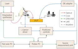
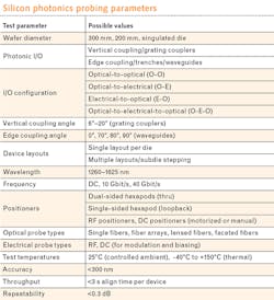
Due to the industry demand for a wide range of applications, flexible probing platforms are needed that can be quickly optimized for the needs of the application. Numerous parameters need to be considered when configuring a prober for one of the applications previously described, along with typical alignment performance requirements in terms of accuracy, throughput, and power coupling repeatability (see table).Each prober configuration is driven by the specific needs of the application. One example of an optical-to-electrical (O-E) probing system configuration setup measures photodiode responsivity, insertion loss, and power coupling efficiency as a function of laser wavelength and state of input polarization (see Fig. 1).
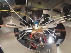
In another configuration, an optical-to-electrical-to-optical (O-E-O) positioner setup is highly directional: optical positioners in the east/west for optical I/O, DC in the south for biasing, and RF in the north for modulation (see Fig. 2). All probes are mounted on motorized positioners for automated indexing between subdie locations with different probing layouts.Alignment methods
Engineering probe systems expose a programmer’s interface to the end user’s Test Executive program, which implements the master control logic for the measurement. The prober’s programming interface enables the master workflow to be tailored to the specific needs of the application. In general, the workflow for a SiPh measurement application consists of the following logic at the master level:
For each wafer
Load/swap wafer from FOUP onto chuck
Align wafer with vision system
For each die
For each subdie structure
Step wafer chuck to subdie
Move positioners to subdie I/O
Move chuck into contact with electrical probes
Align optical probes to device
Perform device measurement
Next subdie
Next die
Next wafer
All the steps in the sequence above are typical and standard to the probing industry, except for the key step Align optical probes to device, which is new. In the optical alignment step, a high-precision alignment with six degrees of freedom (for both translations and rotations) is required to optimize optical power coupling with a given device.
Noncontact optical coupling optimization is critical to minimize insertion loss that will result due to the sensitivity of the alignment error. This contribution to insertion loss is not only a property of the device being tested, but rather involves characteristics of the entire measurement setup, including the probe station and positioning hardware. One key to minimizing loss and performing successful, highly repeatable measurements is to implement a set of calibration functions that compensate for aligning the motion axes of the optical positioners to the motion axes and coordinates of probe station.
To accomplish the optical alignment within performance targets, a specialized 3D piezoelectric actuator and proprietary control algorithms are used. For vertical grating coupler applications, these algorithms include automated move-and-measure control sequences for fiber height control in z, high-speed optical scans in xy, rotation scans in qz, incident angle alignments in qy, gradient searches in xy, and first light search. Similar algorithms are also available for edge coupling applications where the optical signal propagates nominally in the x direction and alignment scans are performed in the yz plane.
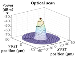
Using an optical scan alignment algorithm, the piezo actuator performs a spiral scan motion about the nominal coupling position on the device while synchronously capturing transmitted power through the device in real time (see Fig. 3). Once the scanning motion completes, the power vs. position data is analyzed in firmware and the fiber is moved to the identified peak. This operation can be accomplished on a two-sided optical-to-optical (O-O) setup within a typical <300 nm accuracy and <3 s alignment time performance target.Once the alignment is complete, the probing system is in a state to take device measurements. Because of the many and varied needs of the application, typically the Test Executive software triggers a measurement routine with the instrumentation such as a wavelength sweep, polarization sweep, s-polarization-parameter measurement, and other user-specific tests. Data is captured on a per-subdie basis and used as appropriate for the application.
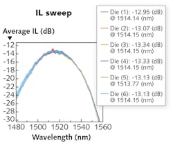
Power coupling can be measured as a function of tunable laser wavelength through a series of insertion loss (IL) wavelength sweep measurements over several devices (see Fig. 4). It is important to note that while the system level calibrations ensure stable measurement repeatability, optical optimization is performed on each device to ensure maximum power transfer.Putting it all together
FormFactor’s wafer probing system, the Cascade CM300xi-SiPh, is engineered as a fully integrated turnkey solution for wafer-level SiPh probing. A wide array of optional hardware, along with industry-exclusive automated system level calibration and alignment routines, both expedite and eliminate the challenge of getting light into and/or out of photonic devices with high precision and application flexibility. Most of the probing parameters discussed previously are supported by our solution, with a long-term roadmap to keep pace with a rapidly evolving industry.
Joe Frankel, Kazuki Negishi, and Mike Simmons are systems engineers in the probe systems division, Dan Rishavy is the market segment director for silicon photonics, and Eric Christenson is the hardware engineering manager of the probe systems division, all at FormFactor, Livermore, CA; e-mail: [email protected]; www.formfactor.com.
