Overcoming inefficiency for quantum light generation
Quantum technologies promise to revolutionize the fields of computing, communications, and sensing. Inherent in realizing this promise is the ability to transmit quantum information. Photons are natural candidates for the task: Unlike other quantum particles, such as electrons, photons interact very weakly with their environment, allowing them to coherently store information while propagating.
Photons are widely used as the basis for the transmission of classical information. Decades of intense research efforts and optimization have produced fiber-optic cables that can transmit photons with extremely low loss—the impact of these discoveries was recognized with the Nobel Prize in Physics in 2009. This low-loss transmission makes fiber-optic cables superior in both transmission distance and bandwidth compared to electrical cables. Fiber-optic connections currently carry the internet; we should anticipate that they will also sustain the “quantum internet” of the future.
An important restriction is that low-loss transmission only works for light in a narrow range of wavelengths, known as the telecom wavelength band. In addition, a key difference with classical technologies is that quantum information needs to be encoded a single photon at a time, requiring specialized techniques for the generation of such photons.
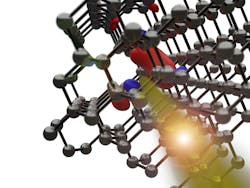
Single photons in a well-defined quantum state can be produced using a variety of sources, but atomic-scale imperfections—“quantum defects”—in crystals have emerged as excellent candidates (see Fig. 1). In contrast to defects in classical devices, which are often detrimental, in the case of quantum defects “the defect is the device” (a phrase coined by the late Audrius Alkauskas, echoing Herbert Kroemer’s famous statement about interfaces). The prototype quantum defect, the nitrogen-vacancy (NV) center in diamond, has already been widely used to demonstrate the fundamental components of a quantum network. But the photons produced by the NV center are in the visible spectrum, far from the desired telecom band. Extensive research efforts have been devoted to finding quantum defects that produce telecom-wavelength photons, but producing single photons with high efficiency has proven challenging.
Our team at the University of California, Santa Barbara, has now uncovered the origin of these difficulties—pointing the way to approaches to surmount them.
Quantum defects as single-photon emitters
The fact that quantum defects are embedded in a crystalline lattice offers many advantages—first and foremost, the ability to manipulate atom-like properties without having to worry about confining atoms in free space. Using the crystalline lattice as a framework for holding the quantum emitter unfortunately also has a downside: Atoms are always in motion, and these vibrations can drain energy away from a quantum defect. This phenomenon is known as electron-phonon coupling, where the electronic states of the defect interact with the vibrations (phonons) of the crystalline lattice.
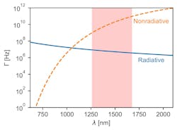
After optical excitation, we expect our quantum defect to emit a photon, but due to electron-phonon coupling, the energy may instead be drained away in the form of phonons. When electron-phonon coupling is strong, this process will severely reduce the efficiency of single-photon emission. Empirically, it had been observed that this efficiency loss becomes more severe at longer wavelengths (towards the telecom band). We focused on developing theoretical methods and simulations that model these processes from first principles, thus developing predictive tools that can explain why the losses so strongly depend on wavelength.
Indeed, our modeling shows that the efficiency decreases exponentially as the emission wavelength increases from the wavelengths of visible light (violet to red) to the infrared wavelengths in the telecom band (see Fig. 2). Importantly, our simulations allow us to identify promising avenues for engineering brighter emitters. Careful choice of the material that hosts the quantum defect is important. In addition, atomic-level engineering of the vibrational properties (both of host and defect) will prove fruitful. We proposed materials such as gallium nitride or aluminum nitride, which are already a technologically mature platform, as promising hosts.
Tackling the efficiency challenge
Another approach involves coupling to a photonic cavity, a topic that benefited from the expertise of Dr. Kamyar Parto and Prof. Galan Moody, collaborators in the UC Santa Barbara Quantum Foundry. When coupled to a photonic cavity, the rate at which a defect emits photons is increased (the so-called Purcell enhancement), while processes enabled by electron-phonon coupling remain constant, and this enhances efficiency.
We should also not solely focus on quantum defects that directly emit at telecom wavelengths. Quantum frequency conversion can be performed with remarkably high efficiency. The ideal emitter might operate at shorter wavelengths, with photons converted to telecom wavelengths prior to transmission.
In our opinion, the “Goldilocks” emitter is still out there. Given the success of the NV center, a great deal of work has focused on diamond as a host material; exploration of alternative host materials is lagging but could prove hugely fruitful.
Overall, the insights provided by our modeling should prove useful for rational design of novel quantum emitters that will ultimately enable long-distance transmission of quantum-encoded information.
FURTHER READING
M. E. Turiansky, K. Parto, G. Moody, and C. G. Van de Walle, APL Photonics, 9, 066117 (Jun. 26, 2024); https://doi.org/10.1063/5.0203366.
About the Author
Mark E. Turiansky
Mark E. Turiansky is a postdoctoral researcher and Quantum Foundry Fellow at the University of California, Santa Barbara.
Chris G. Van de Walle
Chris G. Van de Walle is a distinguished professor and the Herbert Kroemer Chair in Materials Science at the University of California, Santa Barbara. He is also a principal investigator in the Co-design Center for Quantum Advantage, and a Thrust co-leader in the UC Santa Barbara Quantum Foundry.

