Near-field energy transfer provides route to ultrahigh-density solid-state optical memories
With the ever-increasing demand of computational power and memory capacity, we are facing an imminent information bottleneck. As we move from the dimensional to the functional scaling era, it is critical to design novel platforms for information storage and processing.
We propose a new paradigm for an all-optical solid-state memory. In traditional optical memories such as DVD and Blu-ray devices, the volume where a single bit can be stored is limited by the diffraction limit of light. We envision overcoming it by exploiting a dense ensemble of point defects within solids as the information storage medium.1 Specifically, we consider rare earth (RE) ion impurities within an oxide as storage medium.
RE are elements with partially filled and optically active 4f electrons. These 4f electrons are shielded from the environment by the outer filled electrons, which make the RE ions robust against noise and suited for device-level implementations.
For a typical doping concentration, a μm3 volume of material can comprise 10 million RE ions. Each RE ion exhibits slightly different optical emission and absorption energies due to local variations of the crystal field of the host, and each ion can be addressed individually using a narrowband tunable laser, leading to a potential ~1018/cc bit density, comparable to DNA storage. Such density is higher than that of 3D flash memories, the densest memories available today, by 1,000-fold.
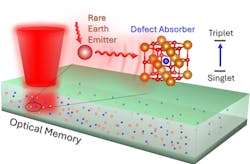
The storage of the bits can be achieved by transferring an optical excitation from the RE ion to a nearby defect in the host crystal, for example an oxygen vacancy or substitutional site. Such transfer processes can occur by nonradiative resonant energy transfer (NRET), and they provide a means to trap excitations into long-lived excited states acting as memory bits. These excited states can then be read out by probing the effect of the energy transfer process on the RE, for example, by optical measurements of the energy or polarization shift of the RE ion (see Fig. 1).
The design of the memories presented above was conceived using a first-principles theoretical and computational framework to understand, qualitatively and quantitatively, NRET processes between defects in solids. By “first principles” we mean the results can be acquired by knowing only the atomic positions within the materials and adopting theories rooted in quantum mechanics—without any need to fit experimental data.
Conventionally, the near-field energy transfer processes between a source and an absorber have been modeled by dipolar transitions between two level systems. However, defects within materials are more complicated. Quantum mechanically, the ground and excited states of the defects are described by many electron wavefunctions, including spin degrees of freedom of all the electrons of the source and absorber. But a detailed quantum mechanical treatment of NRET processes in solids has so far been lacking.
To address this gap, we developed a framework integrating, on the same footing, nonrelativistic quantum electrodynamics (QED) and first-principles electronic structure calculations based on density functional theory (DFT). We describe the light-matter interaction in a form that includes orbital motion and spin degrees of freedom of many electrons at the same time. It allows us to account for the many-body nature of the defect states, and we are able to estimate the rates of the spin-flip and spin-conserving processes individually.
Spin-flip transition at near field
We use our theoretical framework to study an exemplary system: a magnesium oxide (MgO) solid with a neutral oxygen vacancy, also known as an F center (absorber), and implanted RE ions (source). MgO is considered a good host material for spin defects due to its low nuclear spin noise, and the F center is a common and well-understood point defect. The ground state of the F center has two electrons occupying orbitals residing within the band gap of MgO in a singlet configuration; i.e., with zero total spin. An excited state is formed when one of the electrons is excited from a defect orbital resulting in either a singlet excited state (zero spin) or a triplet excited state (spin 1).
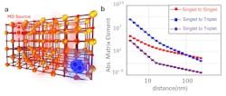
When a far-field photon source, such as a source at a large distance from the defect (e.g., oxygen vacancy or F center), is used for the transition from the ground to an excited state of the F center, only the transition to the singlet excited state is allowed. But when the photon source is in the near field, close to the F center, a transition from the singlet ground to a triplet excited state is not only allowed but can even be stronger than the singlet-to-singlet transition. Such a singlet-to-triplet transition involves a flip of the spin of the electron, which is forbidden at far field (see Fig. 2). It means this triplet excited state can potentially be long lived and used as a memory bit.
Outlook
To enable the design of the ultra-dense optical memories envisioned in our work, we need to enable near-field energy transfer between rare earth impurities and defects, which is responsible for activating spin to triplet long lived transitions. Such transfer requires control over the average spacing between the REs and the defects. A critical parameter to determine is the distance at which the probability of the energy transfer is above of 50%. For the case of the F center within MgO, this distance is found to be a few nanometers—a realistic separation in solid-state systems. Our systematic study not only enables finding such distance parameters but also provides ways to map them as a function of the angle between the RE and the defect.
We emphasize that the NRET processes are ubiquitous within defective semiconductors and insulators, and so they play a role in other quantum technology platforms based on defects within solids. Our framework provides a viable path to a much-needed quantitative understanding of such platforms.
REFERENCE
1. S. Chattaraj, S. Guha, and G. Galli, Phys. Rev. Res., 6, 033170 (2024); https://doi.org/10.1103/physrevresearch.6.033170.
About the Author
Swarnabha Chattaraj
Swarnabha Chattaraj is a postdoctoral appointee in the Materials Science Division at Argonne National Laboratory (Lemont, IL).
Supratik Guha
Supratik Guha is a professor at the University of Chicago’s Pritzker School of Molecular Engineering and senior advisor to Argonne National Laboratory’s Physical Sciences and Engineering.
Giulia Galli
Giulia Galli is a professor of molecular engineering and chemistry at the University of Chicago’s Pritzker School of Molecular Engineering and a senior scientist at Argonne National Laboratory.

