Quantum confinement achieved inside 2D TMD materials
Quantum Innovators: What inspired your quantum nanodot work?
Saiphaneendra Bachu and Nasim Alem: Quantum confinement is the phenomenon where we confine electrons to a small space and they start to behave in a unique way. In such a scenario, they can be used as qubits that are fundamental building blocks of quantum computers. Also, their energy levels become quantized, which means they become a discrete characteristic enabling single-photon emission—useful for quantum communication applications.
Traditionally, quantum confinement is achieved by shrinking materials down to form nanoparticles and quantum dots, which are known as zero-dimensional materials. We wanted to explore whether we could achieve similar confinement inside 2D materials. Our quest to answer this question kickstarted this work (see video).
Quantum Innovators: Can you describe the basic concepts and design work involved? Why 2D materials?
Bachu and Alem: 2D materials are ultrathin sheet-like materials, typically one atom thick, so they are already spatially confined along their thickness direction. A class of 2D materials known as “2D transition metal dichalcogenides (TMDs)” convert from indirect bandgap semiconductors to direct bandgap semiconductors when their thickness is reduced to one atomic layer—and it makes them attractive for light-emitting applications such as light-emitting diodes (LEDs), lasers, etc.
Moreover, light emission efficiency and other electronic and optical properties vary among the family of TMD materials—like molybdenum disulfide (MoS2), tungsten disulfide (WS2), molybdenum diselenide (MoSe2) and tungsten diselenide (WSe2)—because they each have different bandgap energies. By mixing various TMDs (like combining MoSe2 and WSe2 in specific ratios), we can fine-tune the bandgap to emit light at a specific color/energy. This flexibility in band structures makes 2D TMDs an excellent platform for studying and creating light sources, particularly toward quantum applications.
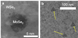
In our work, we formed nanometer-sized islands of 2D MoSe2, nanodots, and embedded them inside a matrix of WSe2 (see Fig. 1). The resulting material is a lateral/in-plane heterostructure and it comprises a nearly continuous WSe2 monolayer interspersed with MoSe2 nanodots of varying sizes under 100 nm. Because of the way the bandgaps of MoSe2 and WSe2 align at the MoSe2/WSe2 interface, all the electrons are localized inside MoSe2, and all the holes are localized in WSe2. The aim of forming this heterostructure is to see if localizing electrons in MoSe2 nanodots can lead to quantum confinement. To detect quantum confinement inside a material, we capture the light emitted by that material and record its energy/wavelength. If the emitted light exhibits higher energy or lower wavelength than normal, it’s a reliable indicator of quantum confinement inside the material.
Quantum Innovators: How does your method work?
Bachu and Alem: To make 2D semiconductor TMD materials emit light, we first need to excite the material using input radiation such as optical lasers or electrons. Upon excitation, these materials form a type of fundamental quasiparticles known as excitons. Excitons are made of an electron and a hole bound together and when they annihilate post-excitation, they emit light. Laser-based optical microscopes are capable of exciting TMD materials toward light emission, but they lack the required spatial resolution to resolve the light emitted from individual MoSe2 nanodots of nanometer size, as is the case in our study.
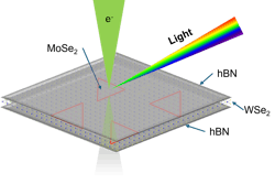
So we used a transmission electron microscope (TEM) equipped with a light detection system to investigate the light emission and potential quantum confinement from MoSe2 nanodots embedded inside WSe2. Briefly, we aim a beam of electrons accelerated at a high voltage inside a TEM to excite the heterostructure and detect the emitted light using a detector. This technique is known as cathodoluminescence (see Fig. 2). Electrons accelerated at high voltages have much smaller wavelengths compared to optical lasers, so the resolution of the instrument is incredibly high, enabling us to resolve light emitted by one nanodot from another nearby dot.
Quantum Innovators: Most surprising/coolest aspects of your work?
Bachu and Alem: One of the initial challenges we faced was that the light emitted from the MoSe2 nanodots was too weak to detect. We brainstormed a few ideas based on previous experience and knowledge from existing scientific literature and increased the intensity of the emitted light by sandwiching the heterostructure between two sheets of hexagonal boron nitride (hBN), which is a wide bandgap insulator that helps provide more electrons and holes to the heterostructure when exposed to electron beam and also improves the efficiency of light emission.
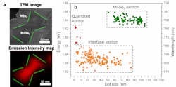
The first time we detected the light emitted by the MoSe2 nanodots and saw that the light is completely localized inside the nanodots, it was a significant breakthrough for our project (see Fig. 3a). We further observed that the light emission from the MoSe2 nanodots strongly depends on the nanodot size wherein the emission is dominated by MoSe2 excitons in dots larger than 85 nm, and by MoSe2/WSe2 interface excitons below 50 nm. Interestingly, at extremely small dot sizes (<10 nm), we observe the energy of the emitted light from interface excitons increases, which is clear evidence of quantum confinement (see Fig. 3b). These results validated our hypothesis that we can localize electrons in spatially confined 2D material nanodots and achieve quantum confinement in 2D nanodots under a threshold size.
Quantum Innovators: What does this mean for quantum computing?
Bachu and Alem: We demonstrated we can confine electrons within the tiniest MoSe2 nanodots and achieve quantum confinement. Also, our results demonstrate that the light emitted by the dots is controlled by the size of the dots. And it should be possible to apply electrostatic gating on the heterostructure to further control the light emission from the nanodots. So our work represents a significant step toward controllably making 2D quantum light sources.
Quantum Innovators: Other applications?
Bachu and Alem: By precisely controlling the excitons in materials, like we did in our study, we can manipulate the light they emit more effectively. This could lead to faster and more secure quantum systems, as well as other customizable, energy-saving devices like higher resolution screen displays.
Quantum Innovators: Any challenges to overcome?
Bachu and Alem: To fully realize the potential of quantum light sources based on 2D nanodots, future work must focus on precise control of size, spatial position, and area density of nanodots. Once we optimize these aspects during the preparation of the nanodot heterostructures, then we need to comprehensively understand how the nanodots interact with each other in terms of light emission so we can produce quantum nanodot displays reliably and consistently.
Quantum Innovators: What’s next?
Bachu and Alem: This study is just the tip of the iceberg. Next, we plan to work on optimizing our synthesis process to achieve precise control over nanodot sizes and expand the study to other family members of TMDs. We also plan to investigate the interaction between nearby nanodots. Overall, by exploring the role of atomic structure, chemistry, and other factors in controlling light emission while expanding on lessons learned in this study, we can move this research to the next level and develop practical applications.
FURTHER READING
S. Bachu et al., ACS Photonics, 12, 1, 364–374 (2024); https://doi.org/10.1021/acsphotonics.4c01739.


