Every problem opens the door to new opportunities. For instance, the ongoing semiconductor chip shortage continues to inspire researchers to look for new, and perhaps better, alternatives to existing approaches.
Case in point? Missouri S&T researchers are demonstrating a new two-dimensional material heterostructure with potential for future applications in “compact sensors and detectors, optical communication, optical integrated circuits and quantum computers.”
As explained in the Nature Portfolio journal, the researchers obtain ultrathin lengenbachite flakes—around 30 nm thick—by mechanically exfoliating the bulk mineral using Nitto PVC tape. The researchers found the strong anisotropic properties of lengenbachite flakes “could have implications for directional light-emitting devices, encrypted data transfer and signal processing, and polarization-sensitive photodetectors.”
“Since the availability of the naturally formed lengenbachite heterostructures is significantly limited, it will be important to successfully grow the corresponding synthetic crystals in order to substantially apply this material into future semiconductor devices,” Dr. Xiaodong Yang, an associate professor of mechanical and aerospace engineering at Missouri S&T and one of the authors of the research paper, tells Laser Focus World. “In recent years, many researchers around the world having been focusing on the exploration and discovery of new types of 2D material heterostructures and their novel functionalities. It is expected some compact 2D heterostructure semiconductor chips will be produced over the next decade.”
According to Yang, “For the mechanical exfoliation of 2D material heterostructures using an adhesive tape, the control of exfoliated flake geometry and precise flake thickness is still technically challenging,” he says. “New techniques need to be developed to achieve exfoliated lengenbachite heterostructures down to monolayer thickness of less than 2 nm in large geometric size.”
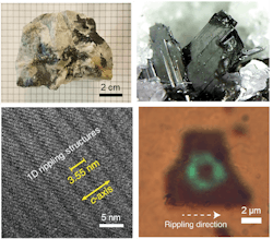
Yang’s team has observed out-of-plane one-dimensional rippling structures along the lengenbachite flake surface. The ripples are caused by the periodic mechanical strain generated between the alternating atomic layers. With the help of several optical spectroscopic techniques, the researchers found strong anisotropic optical properties in the flakes. And, continuing to study the anisotropic mechanical, electrical and magnetic properties of lengenbachite could establish meaningful uses for integrated on-chip sensors and microelectromechanical systems.

Peter Fretty | Market Leader, Digital Infrastructure
Peter Fretty began his role as the Market Leader, Digital Infrastructure in September 2024. He also serves as Group Editorial Director for Laser Focus World and Vision Systems Design, and previously served as Editor in Chief of Laser Focus World from October 2021 to June 2023. Prior to that, he was Technology Editor for IndustryWeek for two years.
As a highly experienced journalist, he has regularly covered advances in manufacturing, information technology, and software. He has written thousands of feature articles, cover stories, and white papers for an assortment of trade journals, business publications, and consumer magazines.
